
Datasheet


MAX7325
I
2
C Port Expander with 8 Push-Pull
and 8 Open-Drain I/Os
9
Maxim Integrated
PIN
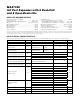
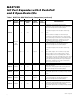
C O NN EC TIO N
DEVICE ADDRESS OUTPUTS POWER-UP DEFAULT
AD2 AD0 A6 A5 A4 A3 A2 A1 A0 O15 O14 O13 O12 O11 O10 O9 O8
SCLGND101000011110000
SCLV+101000111111111
SCLSCL101001011111111
SCLSDA101001111111111
SDAGND101010011110000
SDAV+101010111111111
SDASCL101011011111111
SDASDA101011111111111
GNDGND101100000000000
GNDV+101100100001111
GNDSCL101101000001111
GNDSDA101101100001111
V+GND101110011110000
V+V+101110111111111
V+SCL101111011111111
V+SDA101111111111111
Table 3. MAX7325 Address Map for Outputs O8–O15
Port Inputs
I/O port inputs switch at the CMOS-logic levels as
determined by the expander’s supply voltage, and are
overvoltage tolerant to +6V, independent of the
expander’s supply voltage.
I/O Port Input Transition Detection
All I/O ports configured as inputs are monitored for
changes since the expander was last accessed through
the serial interface. The state of the ports is stored in an
internal “snapshot” register for transition monitoring. The
snapshot is continuously compared with the actual input
conditions, and if a change is detected for any port input,
INT is asserted to signal a state change. The input ports
are sampled (internally latched into the snapshot register)
and the old transition flags cleared during the I
2
C acknowl-
edge of every MAX7325 read and write access. The previ-
ous port transition flags are read through the serial
interface as the second byte of a 2-byte read sequence.