
Datasheet


MAX7325
I
2
C Port Expander with 8 Push-Pull
and 8 Open-Drain I/Os
8
Maxim Integrated
connected to V+ or GND. This is important because the
address selection is used to determine the power-up
logic state and whether pullups are enabled. At power-
up, the I
2
C SDA and SCL bus interface lines are high
impedance at the inputs of every device (master or
slave) connected to the bus, including the MAX7325.
This is guaranteed as part of the I
2
C specification.
Therefore, when address inputs AD0 and AD2 are con-
nected to SDA or SCL during power-up, they appear to
be connected to V+.
The power-up logic uses AD0 to select the power-up
state and whether pullups are enabled for ports P0–P3,
and AD2 for ports P4–P7. The rule is that a logic-high,
SDA, or SCL connection selects the pullups and sets
the default logic state to high. A logic-low deselects the
pullups and sets the default logic state to low (Table 2).
The port configuration is correct on power-up for a
standard I
2
C configuration, where SDA or SCL are
pulled up to V+ by the external I
2
C pullup resistors.
There are circumstances where the assumption that
SDA = SCL = V+ on power-up is not true—for example,
in applications in which there is legitimate bus activity
during power-up. If SDA and SCL are terminated with
pullup resistors to a different supply voltage than the
MAX7325’s supply voltage, and if that pullup supply
rises later than the MAX7325’s supply, then SDA or
SCL may appear at power-up to be connected to GND.
In such applications, use the four address combina-
tions that are selected by connecting address inputs
AD0 and AD2 to V+ or GND (shown in bold in Tables 2
and 3). These selections are guaranteed to be correct
at power-up, independent of SDA and SCL behavior. If
one of the other 12 address combinations is used, an
unexpected combination of pullups might be asserted
until the first I
2
C transmission (to any device, not neces-
sarily the MAX7325) is put on the bus, and an unex-
pected combination of ports can initialize as logic-low
outputs instead of inputs or logic-high outputs.
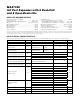
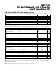
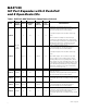
PIN
CONNECTION
DEVICE ADDRESS PORT POWER-UP DEFAULT 40kΩ INPUT PULLUPS ENABLED
AD2 AD0 A6A5A4A3A2A1A0P7P6P5P4P3P2P1P0P7P6P5P4P3P2P1P0
SCLGND110000011110000YYYY————
SCL V+ 110000111111111YYYYYYYY
SCL SCL110001011111111YYYYYYYY
SCL SDA110001111111111YYYYYYYY
SDAGND110010011110000YYYY————
SDA V+ 110010111111111YYYYYYYY
SDA SCL110011011111111YYYYYYYY
SDA SDA110011111111111YYYYYYYY
GNDGND110100000000000————————
GND V+ 110100100001111———— YYYY
GND SCL110101000001111———— YYYY
GNDSDA110101100001111———— YYYY
V+ GND110110011110000YYYY————
V+ V+ 110110111111111YYYYYYYY
V+ SCL110111011111111YYYYYYYY
V+ SDA110111111111111YYYYYYYY
Table 2. MAX7325 Address Map for Ports P0–P7