
Datasheet

On initial power-up, the MAX7322 cannot decode the
address inputs AD2 and AD0 fully until the first I
2
C
transmission. AD0 and AD2 initially appear to be
connected to V+ or GND. This is important because
the address selection determines the power-up logic
state, and whether pullups are enabled. However, at
power-up, the I
2
C SDA and SCL bus interface lines are high
impedance at the pins of every device (master or slave)
connected to the bus, including the MAX7322. This is
guaranteed as part of the I
2
C specification. Therefore,
address inputs AD2 and AD0 that are connected to
SDA or SCL normally appear at power-up to be connect-
ed to V+. The port selection logic uses AD0 to select
whether pullups are enabled for ports I2 and I3, and
to set the initial logic state for ports O0 and O1. AD2
selects whether pullups are enabled for ports I4 and I5
and sets the internal logic state for ports O6 and O7. The
rule is that a logic-high, SDA, or SCL connection selects
the pullups and sets the default logic state high. A logic-
low deselects the pullups and sets the default logic state
low (Table 2). This means that the port configuration is
correct on power-up for a standard I
2
C configuration,
where SDA or SCL are pulled up to V+ by the external I
2
C
pullup resistors.
There are circumstances where the assumption that
SDA = SCL = V+ on power-up is not true—for example,
in applications in which there is legitimate bus activity
during power-up. Also, if SDA and SCL are terminated
with pullup resistors to a different supply voltage than
the MAX7322’s supply voltage, and if that pullup
supply rises later than the MAX7322’s supply, then SDA or
SCL may appear at power-up to be connected to GND.
In such applications, use the four address combina-
tions that are selected by connecting address inputs
AD2 and AD0 to V+ or GND (shown in bold in Table 2).
These selections are guaranteed to be correct at
power-up, independent of SDA and SCL behavior. If
one of the other 12 address combinations is used, an
unexpected combination of pullups might be asserted
until the first I
2
C transmission (to any device, not neces-
sarily the MAX7322) is put on the bus, and an unexpect-
ed combination of ports may initialize as logic-low
outputs instead of inputs or logic-high outputs.
Port Inputs
Port inputs switch at CMOS logic levels as determined
by the expander’s supply voltage, and are overvoltage
tolerant to +6V, independent of the expander’s supply
voltage.
Port Input Transition Detection
All four input ports are monitored for changes since
the expander was last accessed through the serial
interface. The state of the I/O ports is stored in an
internal “snapshot” register for transition monitoring.
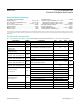
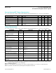
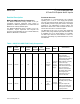
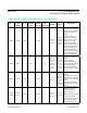
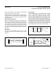
Table 2. MAX7322 Address Map
PIN
CONNECTION
DEVICE ADDRESS OUTPUTS POWER—UP DEFAULT
40kΩ INPUT PULLUPS
ENABLED
AD2 AD0 A6 A5 A4 A3 A2 A1 A0 O7 O6 I5 I4 I3 I2 O1 O0 O7 O6 I5 I4 I3 I2 O1 O0
SCL GND 1 1 0 0 0 0 0 1 1
Inputs
0 0
Pullups are not enabled for push-pull outputs
Y Y — —
Pullups are not enabled for push-pull outputs
SCL V+ 1 1 0 0 0 0 1 1 1 1 1 Y Y Y Y
SCL SCL 1 1 0 0 0 1 0 1 1 1 1 Y Y Y Y
SCL SDA 1 1 0 0 0 1 1 1 1 1 1 Y Y Y Y
SDA GND 1 1 0 0 1 0 0 1 1 0 0 Y Y — —
SDA V+ 1 1 0 0 1 0 1 1 1 1 1 Y Y Y Y
SDA SCL 1 1 0 0 1 1 0 1 1 1 1 Y Y Y Y
SDA SDA 1 1 0 0 1 1 1 1 1 1 1 Y Y Y Y
GND GND 1 1 0 1 0 0 0 0 0 0 0 — — — —
GND V+ 1 1 0 1 0 0 1 0 0 1 1 — — Y Y
GND SCL 1 1 0 1 0 1 0 0 0 1 1 — — Y Y
GND SDA 1 1 0 1 0 1 1 0 0 1 1 — — Y Y
V+ GND 1 1 0 1 1 0 0 1 1 0 0 Y Y — —
V+ V+ 1 1 0 1 1 0 1 1 1 1 1 Y Y Y Y
V+ SCL 1 1 0 1 1 1 0 1 1 1 1 Y Y Y Y
V+ SDA 1 1 0 1 1 1 1 1 1 1 1 Y Y Y Y
www.maximintegrated.com
Maxim Integrated
│
8
MAX7322 I
2
C Port Expander with
4 Push-Pull Outputs and 4 Inputs