
Datasheet


MAX71020
Single-Chip Electricity Meter AFE
7Maxim Integrated
Pin Description
(Pin types: P = Power, O = Output, I = Input, I/O = Input/Output. The circuit number denotes the equivalent circuit, as
specified under Figure 1).
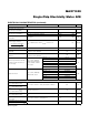
PIN NAME TYPE CIRCUIT DESCRIPTION
POWER AND GROUND PINS
2 GNDA P — Analog Ground. GNDA should be connected directly to the ground plane.
3 V
3P3A
P —
Analog Power Supply. A 3.3V power supply should be connected to
V
3P3A
. V
3P3A
must be the same voltage as V
3P3SYS
.
12 GNDD P — Digital Ground. GNDD should be connected directly to the ground plane.
23 V
DD
O —
Output of the 1.8V Regulator. A 0.1µF bypass capacitor to ground
should be connected to this pin.
24 V
3P3SYS
P —
System 3.3V Supply. V
3P3SYS
should be connected to a 3.3V power
supply.
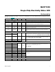
ANALOG PINS
7, 6 IAP, IAN
I 6
Differential or Single-Ended Line Current-Sense Inputs. These pins are
voltage inputs to the internal ADC. Typically, these pins are connected
to the outputs of current sensors. Unused pins must be tied to GNDA.
5, 4 IBP, IBN
1, 28 VA, VB I 6
Line Voltage Sense Inputs. VA/VB are voltage inputs to the internal
ADC. Typically, the pins are connected to the outputs of resistor-
dividers. Unused pins must be tied to GNDA.
25 XIN I
8
Crystal Inputs. A 9.8304MHz crystal should be connected to XIN and
XOUT.
26 XOUT O
DIGITAL PINS
22 DIO0/WPULSE
I/O 3, 4
Multiple-Use Pins. Configurable as DIO. Alternative functions with
proper selection of associated registers are:
DIO0 = WPULSE
DIO1 = VPULSE
21 DIO1/VPULSE
20 DIO2/XPULSE
11 DIO3/YPULSE
8, 27 TEST, TEST0 I 3 Connect to GNDD
9 RESETZ I 3 Active-Low Reset
13 SPI_CSZ I 3
SPI Interface
14 SPI_DO O 4
15 SPI_DI I 3
16 SPI_CLK I 3
19 INTZ O 4 Active-Low Interrupt Request
OTHER PIN
10 V
PP
I — Connect to GNDD