
Datasheet


MAX71020
Single-Chip Electricity Meter AFE
2Maxim Integrated
(All voltages with respect to GNDA.)
Voltage and Current Supplies and Ground Pins
V
3P3SYS
, V
3P3A
..................................................-0.5V to +4.6V
GNDD
...................................................................-0.1V to +0.1V
Analog Input Pins
IAP, IAN, IBP, IBN, VA, VB
............................ (-10mA to +10mA),
(-0.5V to +0.5V)
XIN, XOUT
......................... (-10mA to +10mA), (-0.5V to +3.0V)
Digital Pins
Inputs
.................................... (-10mA to +10mA), (-0.5V to +6V)
Outputs
............ (-10mA to +10mA), (-0.5V to (V
3P3SYS
+ 0.5V))
Temperature and ESD Stress
Operating Junction Temperature (peak, 100ms)
..............140°C
Operating Junction Temperature (continuous)
................. 125°C
Storage Temperature Range
............................ -45°C to +165°C
ESD Stress on All Pins
..............................................±4kV, HBM
Lead Temperature (soldering, 10s)
..................................300°C
Soldering Temperature (reflow)
......................................+250°C
TSSOP
Junction-to-Ambient Thermal Resistance (q
JA
) ..........78°C/W
Junction-to-Case Thermal Resistance (q
JC
) ...............13NC/W
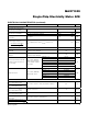
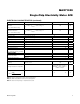
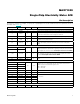
ABSOLUTE MAXIMUM RATINGS
Note 1: Package thermal resistances were obtained using the method described in JEDEC specification JESD51-7, using a four-layer
board. For detailed information on package thermal considerations, refer to www.maximintegrated.com/thermal-tutorial.
Stresses beyond those listed under “Absolute Maximum Ratings” may cause permanent damage to the device. These are stress ratings only, and functional opera-
tion of the device at these or any other conditions beyond those indicated in the operational sections of the specifications is not implied. Exposure to absolute
maximum rating conditions for extended periods may affect device reliability.
PACKAGE THERMAL CHARACTERISTICS (Note 1)
ELECTRICAL CHARACTERISTICS
PARAMETER CONDITIONS MIN TYP MAX UNITS
RECOMMENDED OPERATING CONDITIONS
V
3P3SYS
and V
3P3A
Supply
Voltage
Precision metering operation 3.0 3.6
V
Digital operation (Notes 2, 3) 2.8 3.6
Operating Temperature -40 +85 °C
INPUT LOGIC LEVELS
Digital High-Level Input Voltage
(V
IH
)
2 V
Digital Low-Level Input Voltage
(V
IL
)
0.8 V
Input Pullup Current (I
IL
)
RESETZ
V
V3P3SYS
= 3.6V, V
IN
= 0V 41 78 115 µA
Input Pullup Current (I
IL
) Other
Digital Inputs
V
V3P3SYS
= 3.6V, V
IN
= 0V -1 0 +1 µA
Input Pulldown Current (I
IH
) All
Pins
V
IN
= V
V3P3SYS
-1 0 +1 µA
OUTPUT LOGIC LEVELS
Digital High-Level Output
Voltage (V
OH
)
I
LOAD
= 1mA
V
V3P3SYS
- 0.4
V
I
LOAD
= 15mA (Note 3)
V
V3P3SYS
- 1.1
Digital Low-Level Output
Voltage (V
OL
)
I
LOAD
= 1mA 0 0.4
V
I
LOAD
= 15mA (Note 3) 0 0.96