
Datasheet


Detailed Description
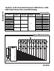
The MAX6979 LED driver comprises a 4-wire serial
interface driving eight constant-current sinking open-
drain output ports. The outputs drive LEDs in either sta-
tic or multiplex applications (Figure 1). The constant-
current outputs are guaranteed for current accuracy
not only with chip-supply voltage variations (5V ±10%
and 3V to 5.5V), but also over a realistic range of driver
output voltage drop (0.5V to 2.5V). The drivers use cur-
rent-sensing feedback circuitry (not simple current mir-
rors) to ensure very small current variations over the full
allowed range of output voltage (see the
Typical
Operating Characteristics
).
MAX6979
16-Port, 5.5V Constant-Current LED Driver with
LED Fault Detection and Watchdog
6 _______________________________________________________________________________________
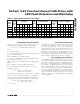
Pin Description
PIN NAME FUNCTION
1 GND Ground
2 DIN Serial-Data Input. Data is loaded into the internal 16-bit shift register on CLK’s rising edge.
3 CLK Serial-Clock Input. Data is loaded into the internal 16-bit shift register on CLK’s rising edge.
4LE
Load-Enable Input. Data is loaded transparently from the internal shift register(s) to the output latch(es)
while LE is high. Data is latched into the output latch(es) on LE's falling edge, and retained while LE is low.
5–20
OUT0–
OUT15
LED Driver Outputs. OUT0 to OUT15 are open-drain, constant-current-sinking outputs rated to 5.5V.
21 OE
Output Enable Input. High forces outputs OUT0 to OUT15 high impedance without altering the contents of
the output latches. Low enables outputs OUT0 to OUT15 to follow the state of the output latches.
22 DOUT Serial-Data Output. Data is clocked out of the 16-bit internal shift register to DOUT on CLK’s rising edge.
23 SET LED Current Setting. Connect SET to GND through a resistor (R
SET
) to set the maximum LED current.
24 V+ Positive Supply Voltage. Bypass V+ to GND with a 0.1µF ceramic capacitor.
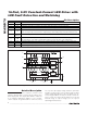
SERIAL-TO-PARALLEL SHIFT REGISTER
LATCHES
OUT0
OUT1
OUT2
DOUT
DIN
CLK
OUT15
CONSTANT-CURRENT SINKS
OUT13
OUT14
POWER-ON
RESET
V+
CURRENT
REFERENCE
V+
OE
GND
GND
LE
D0 D15
D0 D15
D0 D15
R
SET
MAX6979
FAULT DETECTION
WATCH-
DOG
Figure 1. MAX6979 Block Diagram