
Datasheet


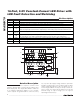

MAX6979
16-Port, 5.5V Constant-Current LED Driver with
LED Fault Detection and Watchdog
2 _______________________________________________________________________________________
ABSOLUTE MAXIMUM RATINGS
Stresses beyond those listed under “Absolute Maximum Ratings” may cause permanent damage to the device. These are stress ratings only, and functional
operation of the device at these or any other conditions beyond those indicated in the operational sections of the specifications is not implied. Exposure to
absolute maximum rating conditions for extended periods may affect device reliability.
Voltage (with respect to GND)
V+ .............................................................................-0.3V to +6V
OUT_ ........................................................................-0.3V to +6V
DIN, CLK, LE, OE, SE ..................................-0.3V to (V+ + 0.3V)
DOUT_ Current .................................................................±10mA
OUT_ Sink Current ..............................................................60mA
Total GND Current ............................................................960mA
Continuous Power Dissipation (T
A
= +70°C)
24-Pin PDIP (derate 13.3mW/°C over +70°C)............1067mW
24-Pin TSSOP (derate 12.2mW/°C over +70°C) .........975mW
Operating Temperature Range .........................-40°C to +125°C
Junction Temperature......................................................+150°C
Storage Temperature Range .............................-65°C to +150°C
Lead Temperature (soldering, 10s) .................................+300°C
Soldering Temperature (reflow)
Lead(Pb)-free packages..............................................+260°C
Packages containing lead(Pb).....................................+240°C
ELECTRICAL CHARACTERISTICS
(
Typical Operating Circuit
, V+ = 3V to 5.5V, T
A
= T
MIN
to T
MAX
, unless otherwise noted. Typical values are at V+ = 5V, T
A
= +25°C.)
(Note 1)
PARAMETER SYMBOL CONDITIONS MIN TYP MAX UNITS
Operating Supply Voltage V+ 3.0 5.5 V
Output Voltage V
OUT
5.5 V
Standby Current
(Interface Idle, All Output Ports
High Impedance, R
SET
= 360Ω)
I
+
All logic inputs at V+ or GND, DOUT
unloaded
5.7 8 mA
Standby Current
(Interface Running, All Output
Ports High Impedance,
R
SET
= 360Ω)
I
+
f
CLK
= 5MHz, OE = V+, DIN and LE = V+
or GND, DOUT unloaded
6 8.5 mA
Supply Current
(Interface Idle, All Output Ports
Active Low, R
SET
= 360Ω)
I
+
All logic inputs at V+ or GND,
DOUT unloaded
18 25 mA
Input High Voltage
DIN, CLK, LE, OE
V
IH
0.7 x
V+
V
Input Low Voltage
DIN, CLK, LE, OE
V
IL
0.3 x
V+
V
Hysteresis Voltage
DIN, CLK, LE, OE
∆V
I
0.8 V
Input Leakage Current
DIN, CLK, LE, OE
I
IH
, I
IL
-1 +1 µA
Output High Voltage DOUT V
OH
I
SOURCE
= 4mA
V +
- 0.5V
V
Output Low Voltage V
OL
I
SINK
= 4mA 0.5 V
Output Current OUT I
OUT
V+ = 3V to 5.5V, V
OUT
= 0.5V to 2.5V,
R
SET
= 360Ω
37 50 61 mA
Output Leakage Current OUT I
LEAK
OE = V+, V
OUT
= V+ 1 µA
Watchdog Timeout t
WD
0.1 1 2.5 s