
Datasheet
MAX6968
8-Port, 5.5V Constant-Current LED Driver
6 _______________________________________________________________________________________
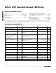
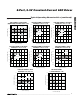
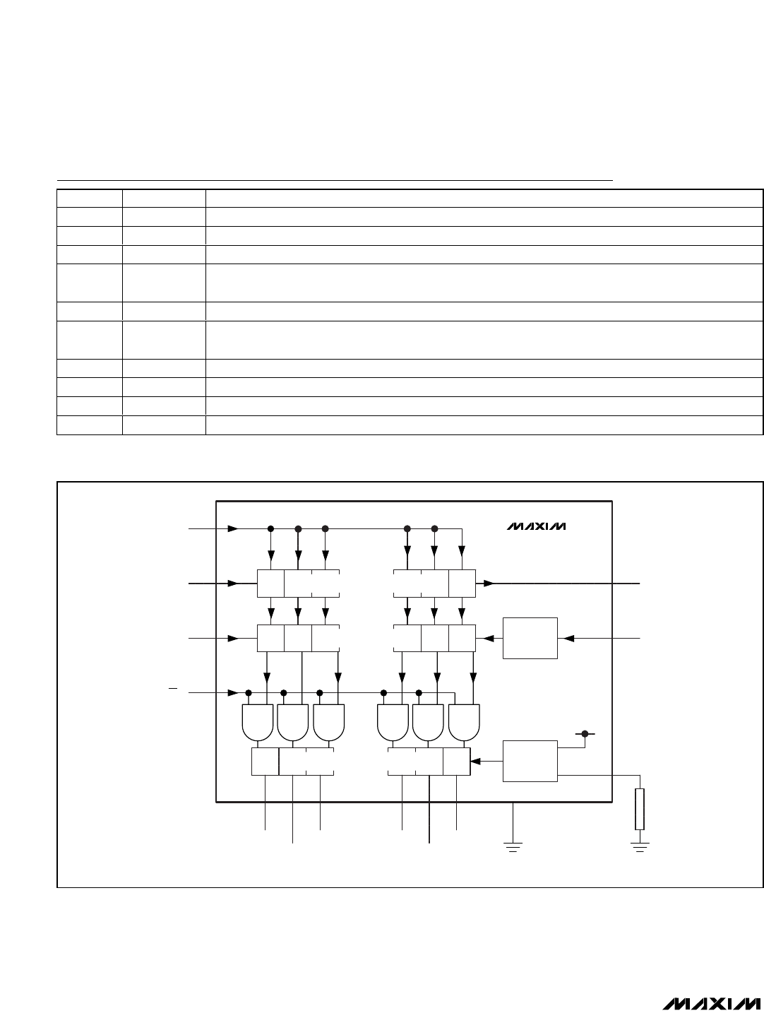
Pin Description
PIN NAME FUNCTION
1 GND Ground
2 DIN Serial-Data Input. Data is loaded into the internal 8-bit shift register on CLK’s rising edge.
3 CLK Serial-Clock Input. Data is loaded into the internal 8-bit shift register on CLK’s rising edge.
4LE
Load-Enable Input. Data is loaded transparently from the internal shift register to the output latch while
LE is high. Data is latched into the output latch on LE's falling edge, and retained while LE is low.
5–12
OUT0–OUT7
LED Driver Outputs. OUT0–OUT7 are open-drain, constant-current sinking outputs rated to 5.5V.
13 OE
O utp ut- E nab l e Inp ut. H i g h for ces outp uts OUT0–OUT7 to hi g h i m p ed ance, w i thout al ter i ng the contents of
the outp ut l atches. Low enab l es outp uts OUT0–OUT7 to fol l ow the state of the outp ut l atches.
14 DOUT
Serial-Data Output. Data is clocked out of the 8-bit internal shift register to DOUT on CLK’s rising edge.
15 SET LED Current Setting. Connect SET to GND through a resistor (R
SET
) to set the maximum LED current.
16 V+ Positive Supply Voltage. Bypass V+ to GND with a 0.1µF ceramic capacitor.
PAD
E xp osed p ad *
Exposed pad on package underside. Connect to GND.
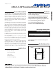
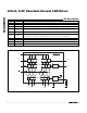
SERIAL-TO-PARALLEL SHIFT REGISTER
LATCHES
OUT0
OUT1
OUT2
DOUTDIN
CLK
OUT7
CONSTANT-CURRENT SINKS
OUT5
OUT6
POWER-ON
RESET
V+
CURRENT
REFERENCE
V+
OE
GND GND
LE
D0 D7
D0 D7
D0 D7
R
SET
MAX6968
Figure 1. MAX6968 Block Diagram
*TSSOP package only.