
Datasheet

MAX6960–MAX6963
4-Wire Serially Interfaced
8 x 8 Matrix Graphic LED Drivers
23
Maxim Integrated
Current Plane Identification (Bits D2, D3)
The current plane bits in the global panel configuration
register identify which memory plane is currently being
used to control the display panel (Table 18). These bits
are read only; written data is ignored.
Ripple Sync (Bit D4)
The ripple sync feature, when enabled in the global panel
configuration register, desynchronizes the multiplex timing
of all the interconnected MAX6960 drivers on a display
panel by OSC/4 (Table 19). This delay spreads the drive
transitions among the drivers to spread power-supply
peak-current demand, and ease decoupling. The maxi-
mum delay from first driver to last driver is 244µs with the
maximum of 256 drivers used. This is too short a time to
cause visible artifacts.
Mux Flip (Bit D5)
The mux flip feature in the global panel configuration reg-
ister reverses the panel PWM timing for alternate drivers
when enabled (Table 20). Again, this spreads power-sup-
ply peak-current demand.
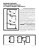
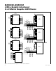
Color Control (Bit D6)
The color control bit in the global panel configuration reg-
ister selects whether a monocolor or RGY display panel is
built. Select monocolor when building an RGB panel as
shown in Figure 17. This bit is fixed at zero for the
MAX6962 and MAX6963, and a write to this bit is ignored
for these parts.
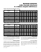
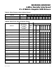
REGISTER DATA
REGISTER
ADDRESS
CODE (HEX)
D7 D6 D5 D4 D3 D2 D1 D0
0/256 0x03 0 0 0 0000 0
1/256 0x03 0 0 0 0000 1
2/256 0x03 0 0 0 0001 0
3/256 0x03 0 0 0 0001 1
4/256 0x03 0 0 0 0010 0
— 0x03 ————————
251/256 0x03 1 1 1 1101 1
252/256 0x03 1 1 1 1110 0
253/256 0x03 1 1 1 1110 1
254/256 0x03 1 1 1 1111 0
255/256 (max on) 0x03 1 1 1 1111 1
Table 25. Digit 0 Intensity Register Format
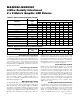
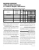
REGISTER DATA
REGISTER
ADDRESS CODE
(HEX)
D7 D6 D5 D4 D3 D2 D1 D0
0/256 0x04 0 0 000000
1/256 0x04 0 0 000001
2/256 0x04 0 0 000010
3/256 0x04 0 0 000011
4/256 0x04 0 0 000100
— 0x04 ————————
251/256 0x04 1 1 111011
252/256 0x04 1 1 111100
253/256 0x04 1 1 111101
254/256 0x04 1 1 111110
255/256 (max on) 0x04 1 1 111111
Table 26. Digit 1 Intensity Register Format