
Datasheet
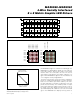

MAX6960–MAX6963
4-Wire Serially Interfaced
8 x 8 Matrix Graphic LED Drivers
2
Maxim Integrated
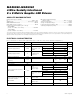
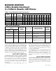
ABSOLUTE MAXIMUM RATINGS
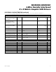
ELECTRICAL CHARACTERISTICS
(V+ = 2.7V to 3.6V, T
A
= T
MIN
to T
MAX
, typical values at V+ = 3.3V, T
A
= +25°C, unless otherwise noted.) (Note 1)
Stresses beyond those listed under “Absolute Maximum Ratings” may cause permanent damage to the device. These are stress ratings only, and functional
operation of the device at these or any other conditions beyond those indicated in the operational sections of the specifications is not implied. Exposure to
absolute maximum rating conditions for extended periods may affect device reliability.
(Voltage with respect to GND.)
V+ .............................................................................-0.3V to +4V
All Other Pins................................................-0.3V to (V+ + 0.3V)
ROW1–ROW8 Sink Current ..............................................750mA
COL1–COL16 Source Current ...........................................48mA
Continuous Power Dissipation (T
A
= +70°C)
44-Pin MQFP
(derate 12.7 mW/°C over +70°C)...............................1012mW
44-Pin TQFN
(derate 27mW/°C over +70°C)...................................2162mW
Operating Temperature Range
(T
MIN
to T
MAX
) ..............................................-40°C to +125°C
Junction Temperature......................................................+150°C
Storage Temperature Range .............................-65°C to +150°C
Lead Temperature (soldering, 10s) .................................+300°C
Soldering Temperature (reflow) .......................................+240°C
PARAMETER SYMBOL CONDITIONS MIN TYP MAX UNITS
Operating Supply Voltage V+ 2.7 3.6 V
T
A
= +25°C 250 375
T
A
= T
MIN
to +85°C 500Shutdown Supply Current I
SHDN
Shutdown mode, all
digital inputs at V+
or GND
T
A
= T
MIN
to T
MAX
600
µA
T
A
= +25°C 7.5 9
T
A
= T
MIN
to +85°C 10Operating Supply Current I+
Intensity set to full,
no display load
connected
T
A
= T
MIN
to T
MAX
11
mA
Master Clock Frequency f
OSC
1.0 8.5 MHz
Dead-Clock Protection
Frequency
f
OSC
50 90.5 200 kHz
OSC High Time t
CH
40 ns
OSC Low Time t
CL
40 ns
T
A
= +25°C 38 40 42
T
A
= T
MIN
to +85°C 37 43
V
LED
= 2.3V, V+ =
3.15V to 3.6V,
current = high
T
A
= T
MIN
to T
MAX
37 44
T
A
= +25°C 19 20 21
T
A
= T
MIN
to +85°C 18.5 21.5
Anode Column Source Current
COL1–COL16
I
SEG
V
LED
= 2.3V, V+ =
2.7V to 3.6V, current
= low
T
A
= T
MIN
to T
MAX
18.5 22.0
mA
V
LED
= 2.3V, V+ = 3.15V to 3.6V,
current = high
200
Anode Column Source-Current
Temperature Variation
COL1–COL16
I
TC
V
LED
= 2.2V, V+ = 2.7V to 3.3V,
current = low
200
ppm/°C
Segment Current Slew Rate ∆I
SEG
/∆tT
A
= +25°C 30 mA/µs