
Datasheet

MAX6960–MAX6963
4-Wire Serially Interfaced
8 x 8 Matrix Graphic LED Drivers
15
Maxim Integrated
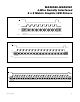
3-Wire Interface Data Lines
(ADDOUT and ADDIN)
One MAX6960 is designated the master device, and this
is allocated driver address 0. The master’s ADDIN pin is
connected to V+, identifying it as the first device. This
first MAX6960 should be the driver for the top-left pix-
els of the display panel. The master’s
ADDOUT pin is connected to the second MAX6960’s
ADDIN pin, and that MAX6960’s ADDOUT pin is connect-
ed to the third MAX6960’s ADDIN, and so on up to 256
MAX6960s. The last MAX6960’s ADDOUT pin is left open
circuit. The last MAX6960 should be the driver for the
bottom-right pixels of the display panel. The ADDOUT
is initialized low at the start of a 3-wire interface configura-
tion operation, and goes high (N + 1.5) ADDCLK periods
later, where n is the driver address of the MAX6960 (0 to
255). See Figures 1 and 2 for connection examples.
3-Wire Interface Clock (ADDCLK)
The ADDCLK pins for all MAX6960s are all connected
together. ADDCLK data rate is determined by OSC / 4,
nominally 1.048576 MHz. The ADDCLK pin for the master
MAX6960 (driver address 0) is always an output, and all
the other ADDCLKs are always inputs. ADDCLK is active
for exactly 256 clock cycles when a panel configuration is
being performed (on power-up reset, and after a write to
the global panel configuration register).
Use of ADDOUT as Plane Change Interrupt
(IRQ)
When the plane counter is configured to automatic mode
(bit 6 of the global plane counter register is set) (Table
30), ADDOUT pulses low for a time of 512/OSC (nominally
122µs) at the start of every automatic plane change. This
signal can be used as an interrupt output from the display
panel to the host to flag that the previous display plane is
now unused and can be written with a new image.
Multiplex Clock
The OSC input for all MAX6960s sharing a 3-wire interface
bus (but not necessarily a 4-wire interface bus) should be
driven by a common CMOS-level clock ranging between
1MHz and 8.5MHz. It is usually necessary to use an exter-
nal clock tree to fan out multiple clock drives when larger
numbers of MAX6960s are used because of the capaci-
tive loads. For example, each one of the eight outputs of a
standard 74HC541 octal buffer could drive 8 to 32
MAX6960 OSC inputs, depending on the layout used.
The recommended setting for OSC is 4.194303MHz. This
frequency sets the slow global plane counter resolution to
1s, and the fast global plane counter resolution to 1Hz.
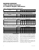
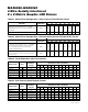
COMMAND ADDRESS
REGISTER
D15 D14 D13 D12 D11 D10 D9 D8
HEX CODE
Driver Address (read only) X X 0000 0x00
Pixel Intensity Scale X 0001 0x01
Panel Intensity X 0010 0x02
Digit 0 Intensity X 0011 0x03
Digit 1 Intensity X 0100 0x04
Fault X 0101 0x05
— X0110 0x06
—
Autoincrement
Local/Global
X0111 0x07
Global Driver Indirect Address* X X X 1000 0x08
Global Display Indirect Address LSB* X X X 1001 0x09
Global Display Indirect Address
XXX1010 0x0A
Global Plane Counter* X X X 1011 0x0B
Global Clear Planes* X X X 1100 0x0C
Global Panel Configuration* X X X 1101 0x0D
Global Driver Devices*
R/W
XXX1110 0x0E
Global Driver Rows* X X X 1111 0x0F
Table 8. Register Address Map
*
When reading from the global registers, only the master MAX6960 (whose driver address is 0x00) responds.