
Datasheet


A logic-high selects hexadecimal decoding, while a
logic-low bypasses the decoder. When direct control is
selected, the data bits D7 to D0 correspond to the seg-
ment lines of the MAX6954. Write x0010000 to blank all
segments in hexadecimal decode mode.
Display Blink Mode
The display blinking facility, when enabled, makes the
driver flip automatically between displaying the digit reg-
ister data in planes P0 and P1. If the digit register data
for any digit is different in the two planes, then that digit
appears to flip between two characters. To make a char-
acter appear to blink on or off, write the character to one
plane, and use the blank character (0x20) for the other
plane. Once blinking has been configured, it continues
automatically without further intervention.
Blink Speed
The blink speed is determined by the frequency of the
multiplex clock, OSC, and by the setting of the Blink Rate
Selection Bit B (Table 18) in the configuration register.
The Blink Rate Selection Bit B sets either fast or slow
blink speed for the whole display.
Initial Power-Up
On initial power-up, all control registers are reset, the
display is blanked, intensities are set to minimum, and
shutdown is enabled (Table 15).
Conguration Register
The configuration register is used to enter and exit shut-
down, select the blink rate, globally enable and disable
the blink function, globally clear the digit data, select
between global or digit-by-digit control of intensity, and
reset the blink timing (Tables 16–19 and 21–24).
The configuration register contains 7 bits:
● S bit selects shutdown or normal operation (read/write).
● B bit selects the blink rate (read/write).
● E bit globally enables or disables the blink function
(read/write).
● T bit resets the blink timing (data is not stored—tran-
sient bit).
● R bit globally clears the digit data for both planes P0
and P1 for ALL digits (data is not stored—transient
bit).
● I bit selects between global or digit-by-digit control
of intensity (read/write).
● P bit returns the current phase of the blink timing
(read only—a write to this bit is ignored).
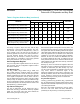
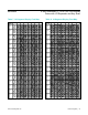
Character Generator Font Mapping
The font is composed of 104 characters in ROM. The
lower 7 bits of the 8-bit digit register represent the char-
acter selection. The most significant bit, shown as x in the
ROM map of Tables 7 and 8, is 1 to light the DP segment
and zero to leave the DP segment unlit.
The character map follows the standard ASCII font for
96 characters in the x0101000 through x1111111
range. The first 16 characters of the 16-segment ROM
map cover 7-segment displays. These 16 characters
are numeric 0 to 9 and characters A to F (i.e., the hexa-
decimal set).
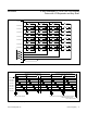
Multiplex Clock and Blink Timing
The OSC pin can be fitted with capacitor C
SET
to GND
to use the internal RC multiplex oscillator, or driven by an
external clock to set the multiplex clock frequency and
blink rate. The multiplex clock frequency determines the
frequency that the complete display is updated. With OSC
at 4MHz, each display digit is enabled for 200µs.
The internal RC oscillator uses an external resistor, R
SET
,
and an external capacitor, C
SET
, to set the oscillator fre-
quency. The suggested values of R
SET
(56kW) and C
SET
(22pF) set the oscillator at 4MHz, which makes the blink
frequency 0.5Hz or 1Hz.
The external clock is not required to have a 50:50 duty
cycle, but the minimum time between transitions must
be 50ns or greater and the maximum time between
transitions must be 750ns.
The on-chip oscillator may be accurate enough for appli-
cations using a single device. If an exact blink rate is
required, use an external clock ranging between 1MHz
and 8MHz to drive OSC. The OSC inputs of multiple
MAX6954s can be tied together to a common external
clock to make the devices blink at the same rate. The
relative blink phasing of multiple MAX6954s can be syn-
chronized by setting the T bit in the control register for all
the devices in quick succession. If the serial interfaces of
multiple MAX6954s are daisy-chained by connecting the
DOUT of one device to the DIN of the next, then synchro-
nization is achieved automatically by updating the config-
uration register for all devices simultaneously. Figure 6 is
the multiplex timing diagram.
OSC_OUT Output
The OSC_OUT output is a buffered copy of either the
internal oscillator clock or the clock driven into the OSC
pin if the external clock has been selected. The feature
is useful if the internal oscillator is used, and the user
wishes to synchronize other MAX6954s to the same
blink frequency. The oscillator is disabled while the
MAX6954 is in shutdown.
www.maximintegrated.com
Maxim Integrated
│
11
MAX6954 4-Wire Interfaced, 2.7V to 5.5V LED Display
Driver with I/O Expander and Key Scan