
Datasheet


Operation Without a Backup Power Source
If a backup power source is not used, ground V
BATT
and
connect V
OUT
to V
CC
. Since there is no need to switch
over to any backup power source, V
OUT
does not need
to be switched. A direct connection to V
CC
eliminates any
voltage drops across the switch which may push V
OUT
below V
CC
.
Replacing the Backup Battery
The backup battery can be removed while V
CC
remains
valid, without danger of triggering RESET/RESET. As
long as V
CC
stays above the reset threshold, battery-
backup mode cannot be entered. In other switchover ICs
where battery-backup mode is entered whenever V
BATT
gets close to V
CC
, an unconnected V
BATT
pin accumu-
lates leakage charge and triggers RESET/RESET in error.
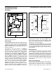
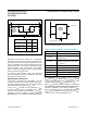
Adding Hysteresis to the Power-Fail
Comparator
Hysteresis adds a noise margin to the power-fail
comparator and prevents repeated triggering of PFO
when V
IN
is close to its trip point. Figure 6 shows how to
add hysteresis to the power-fail comparator. Select the
ratio of R
1
and R
2
such that PFI sees 1.25V when V
IN
falls to its trip point (V
TRIP
). R
3
adds the hysteresis. It will
typically be an order of magnitude greater than R
1
or R
2
(about 10 times either R
1
or R
2
). The current through R
1
and R
2
should be at least 1μA to ensure that the 25nA
(max) PFI input current does not shift the trip point. R
3
should be larger than 10kΩ so it does not load down the
PFO pin. Capacitor C1 adds additional noise rejection.
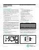
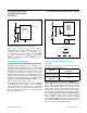
Monitoring a Negative Voltage
The power-fail comparator can be used to monitor a
negative supply rail using the circuit of Figure 7. When
the negative rail is good (a negative voltage of large mag-
nitude), PFO is low. When the negative rail is degraded
(a negative voltage of lesser magnitude), PFO goes high.
This circuit’s accuracy is affected by the PFI threshold
tolerance, the V
CC
line, and the resistors.
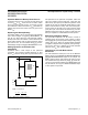
Interfacing to μPs with Bidirectional
Reset Pins
μPs with bidirectional reset pins, such as the Motorola
68HC11 series, can contend with the MAX690A/MAX692A/
MAX802L/MAX802M RESET output. If, for example, the
RESET output is driven high and the μP wants to pull it
low, indeterminate logic levels may result. To correct this,
connect a 4.7kΩ resistor between the RESET output and
the μP reset I/O, as in Figure 8. Buffer the RESET output
to other system components.
Figure 7. Monitoring a Negative Voltage
PFO
V
CC
GND
MAX690A
MAX692A
MAX802L
MAX802M
MAX805L
+5V
R
2
R
1
PFI
+5V
0V
PFO
V
TRIP
V-
0V
V-
NOTE: V
TRIP
IS NEGATIVE
R
1
+
V
L
- 1.25
R
2
1.25 - V
TRIP
MAX690A/MAX692A/
MAX802L/MAX802M/
MAX805L
Microprocessor Supervisory Circuits
www.maximintegrated.com
Maxim Integrated
│
9