
Datasheet

Terminal Voltage (with respect to GND)
V
CC1
, V
CC2
.........................................................-0.3V to +6V
Open-Drain RST, RST1, RST2, PFO, RST ............-0.3V to +6V
Push-Pull RST, RST1, PFO, RST .......... -0.3V to (V
CC1
+ 0.3V)
Push-Pull RST2 ...................................... -0.3V to (V
CC2
+ 0.3V)
RSTIN, PFI, MR, WDI .............................................-0.3V to +6V
Input Current/Output Current (all pins) ...............................20mA
Continuous Power Dissipation (T
A
= +70°C)
5-Pin SOT23-5 (derate 7.1mW/°C above +70°C) .......571mW
6-Pin SOT23-6 (derate 8.7mW/°C above +70°C) .......696mW
8-Pin SOT23-8 (derate 8.9mW/°C above +70°C) .......714mW
Operating Temperature Range ......................... -40°C to +125°C
Storage Temperature Range ............................ -65°C to +150°C
Junction Temperature ......................................................+150°C
Lead Temperature (soldering, 10s) .................................+300°C
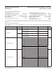
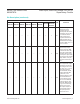
(V
CC1
= 0.8V to 5.5V, V
CC2
= 0.8V to 5.5V, GND = 0V, T
A
= -40°C to +125°C, unless otherwise noted. Typical values are at T
A
=
+25°C.) (Note 1)
PARAMETER SYMBOL CONDITIONS MIN TYP MAX UNITS
Supply Voltage V
CC
0.8 5.5 V
Supply Current
I
CC1
V
CC1
< 5.5V all I/O connections open,
outputs not asserted
15 39
µA
V
CC1
< 3.6V all I/O connections open,
outputs not asserted
10 28
I
CC2
V
CC2
< 3.6V all I/O connections open,
outputs not asserted
4 11
V
CC2
< 2.75V all I/O connections open,
outputs not asserted
3 9
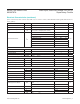
V
CC1
Reset Threshold V
TH1
L (falling) 4.500 4.625 4.750
V
M (falling) 4.250 4.375 4.500
T (falling) 3.000 3.075 3.150
S (falling) 2.850 2.925 3.000
R (falling) 2.550 2.625 2.700
Z (falling) 2.250 2.313 2.375
Y (falling) 2.125 2.188 2.250
W (falling) 1.620 1.665 1.710
V (falling) 1.530 1.575 1.620
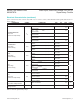
V
CC2
Reset Threshold V
TH2
T (falling) 3.000 3.075 3.150
V
S (falling) 2.850 2.925 3.000
R (falling) 2.550 2.625 2.700
Z (falling) 2.250 2.313 2.375
Y (falling) 2.125 2.188 2.250
W (falling) 1.620 1.665 1.710
V (falling) 1.530 1.575 1.620
I (falling) 1.350 1.388 1.425
H (falling) 1.275 1.313 1.350
G (falling) 1.080 1.110 1.140
F (falling) 1.020 1.050 1.080
E (falling) 0.810 0.833 0.855
D (falling) 0.765 0.788 0.810
MAX6715A–MAX6729A/
MAX6797A
Dual/Triple, Ultra-Low-Voltage, SOT23 μP
Supervisory Circuits
www.maximintegrated.com
Maxim Integrated
│
2
Absolute Maximum Ratings
Stresses beyond those listed under “Absolute Maximum Ratings” may cause permanent damage to the device. These are stress ratings only, and functional operation of the device at these
or any other conditions beyond those indicated in the operational sections of the specifications is not implied. Exposure to absolute maximum rating conditions for extended periods may affect
device reliability.
Electrical Characteristics