
Datasheet
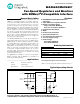


Fan-Speed Regulators and Monitors
with SMBus/I
2
C-Compatible Interface
2 Maxim Integrated
MAX6650/MAX6651
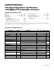
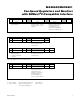
ABSOLUTE MAXIMUM RATINGS
ELECTRICAL CHARACTERISTICS
(V
CC
= 3.0V to 5.5V, T
A
= -40°C to +85°C, unless otherwise noted. Typical values are at T
A
= +25°C and V
CC
= 5V.)
Stresses beyond those listed under “Absolute Maximum Ratings” may cause permanent damage to the device. These are stress ratings only, and functional
operation of the device at these or any other conditions beyond those indicated in the operational sections of the specifications is not implied. Exposure to
absolute maximum rating conditions for extended periods may affect device reliability.
V
CC
to GND..............................................................-0.3V to +6V
FB, TACH_ ..........................................................-0.3V to +13.2V
All Other Pins..............................................-0.3V to (V
CC
+ 0.3V)
Output Voltages..........................................-0.3V to (V
CC
+ 0.3V)
Maximum Current
Into V
CC
, GND, V
OUT
...................................................100mA
Into All Other Pins ..........................................................50mA
Continuous Power Dissipation (T
A
= +70°C)
µMAX (derate 5.6mW/°C above +70°C) .....................444mW
QSOP (derate 8.3mW/°C above +70°C).....................667mW
Operating Temperature Range ...........................-40°C to +85°C
Junction Temperature .....................................................+150°C
Storage Temperature Range .............................-65°C to +150°C
Lead Temperature (soldering, 10s) .................................+300°C
Soldering Temperature (reflow)
Lead(Pb)-free..............................................................+260°C
Containing lead(Pb) ....................................................+240°C
Input Low Voltage
Input Hysteresis V
HYS
200 mV
Tachometer Threshold V
TACH_
V
FB
+ 1.0 V
FB
+3
V
12V fan, 0 < V
FB
< 9V
PARAMETER SYMBOL MIN TYP MAX UNITS
Output Source Current I
SOURCE
50 mA
Output Sink Current I
SINK
10 mA
Output Voltage Range V
OUT
0.3 V
CC
- 0.3 V
V
FB
+ 0.5 V
FB
+1.5
Tachometer Input Impedance R
TACH_
70 100 150 kΩ
Supply Voltage V
CC
3.0 5.5 V
Supply Current I
CC
10 mA
DAC Differential Nonlinearity 5 LSB
Useful DAC Resolution 8 bits
Feedback Input Impedance R
FB
70 100 150 kΩ
Output Sink Current I
GPIO_
10 mA
CONDITIONS
Guaranteed monotonicity on FB (Note 1)
V
OUT
= V
CC
- 1.8V
Measured at FB (Note 1)
V
OUT
= 0.5V
I
OUT
= ±100µA
5V fan, 0 < V
FB
< 4.5V
0 < VFB < 9V
0 < V
TACH
< 9V
V
GPIO_
= 0.4V
Full-on mode, I
OUT
= 0
V
0.8V
IL(GPIO_)
Input High Voltage
V
2V
CC
≤ 3.6V
V
IH(GPIO_)
3V
CC
> 3.6V
Pullup Resistor R
GPIO_
100 kΩ
TACHOMETER INPUTS (TACH_)
FEEDBACK (FB)
GENERAL-PURPOSE INPUTS/OUTPUTS (GPIO_) (Note 2)
POWER SUPPLY (V
CC
)
OUTPUT (OUT)