
Datasheet

MAX5902/MAX5903
+72V, SOT23/TDFN, Simple Swapper Hot-Swap
Controllers
_______________________________________________________________________________________ 3
Note 1: All currents into device pins are positive, all currents out of device pins are negative, and all voltages are referenced to
GND, unless otherwise noted.
Note 2: All specifications are 100% tested at T
A
= +25°C, unless otherwise noted. Specifications over -40°C to +85°C are guaran-
teed by characterization.
Note 3: This is the delay time from a valid on condition until V
GS
begins rising. Valid on conditions are: the device is not in undervolt-
age lockout; ON/OFF is not driven low; and the device is not in thermal shutdown.
Note 4: This is the delay from a valid low on ON/OFF until V
GS
falls. Pulses on ON/OFF less than t
OFF
are ignored, offering glitch
immunity.
Note 5: Guaranteed by characterization, not production tested. C
GATE
is a capacitor from GATE to V
S
.
ELECTRICAL CHARACTERISTICS (continued)
(V
S
= +9V to +72V, GND = 0V, ON/OFF open circuit, T
A
= -40°C to +85°C, unless otherwise noted. Typical values are at V
S
= +48V
and T
A
= +25°C.) (Notes 1, 2)
PARAMETER
SYM B O L
C O ND IT IO N S
M IN
T YP
M A X
U N IT S
Power-Good Output Open-Drain
Leakage Current
I
OH
V
PGOOD
= 72V (MAX5902)
V
PGOOD
= 72V (MAX5903)
10 µA
Thermal Shutdown Temperature
T
SD
Junction temperature
+125
°C
Thermal Shutdown Hysteresis
T
HY
15 °C
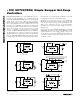
Typical Operating Characteristics
(V
S
= +48V, GND = 0V, and T
A
= +25°C, unless otherwise noted. See Figure 2 for test circuits.)
0.7
0.8
1.0
0.9
1.1
1.2
03015 45 60 75
SUPPLY CURRENT
vs. INPUT VOLTAGE
MAX5902 toc01
INPUT VOLTAGE (V)
SUPPLY CURRENT (mA)
0.7
0.8
1.0
0.9
1.1
1.2
-40 10-15 35 60 85
SUPPLY CURRENT
vs. TEMPERATURE
MAX5902 toc02
TEMPERATURE (°C)
SUPPLY CURRENT (mA)
V
IN
= +70V
V
IN
= +48V
V
IN
= +12V
25
28
27
26
29
30
31
32
33
34
35
-40 10-15 356085
V
UVLO
THRESHOLD
vs. TEMPERATURE
MAX5902 toc03
TEMPERATURE (°C)
LOCKOUT VOLTAGE (V)
INCREASING V
IN
DECREASING V
IN