
Datasheet

MAX5902/MAX5903
+72V, SOT23/TDFN, Simple Swapper Hot-Swap
Controllers
2 _______________________________________________________________________________________
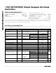
ABSOLUTE MAXIMUM RATINGS
ELECTRICAL CHARACTERISTICS
(V
S
= +9V to +72V, GND = 0V, ON/OFF open circuit, T
A
= -40°C to +85°C, unless otherwise noted. Typical values are at V
S
= +48V
and T
A
= +25°C.) (Notes 1, 2)
Stresses beyond those listed under “Absolute Maximum Ratings” may cause permanent damage to the device. These are stress ratings only, and functional
operation of the device at these or any other conditions beyond those indicated in the operational sections of the specifications is not implied. Exposure to
absolute maximum rating conditions for extended periods may affect device reliability.
Terminal Voltage (with respect to GND unless otherwise noted)
V
S
, DRAIN, PGOOD, PGOOD ................................-0.3V to +76V
ON/OFF ....................................................................-0.3V to +4V
GATE to V
S
............................................................-12V to +0.3V
Current into any Pin ............................................................±3mA
Continuous Power Dissipation (T
A
= +70°C)
6-Pin SOT23 (derate 9.1mW/°C above +70°C)..........727mW
6-Pin TDFN (derate 18.2mW/°C above +70°C) .......1454mW
Junction to Case
Thermal Resistance, θ
JC
(TDFN) ..............................8.5°C/W
Maximum Junction Temperature .....................................+150°C
Storage Temperature Range .............................-60°C to +150°C
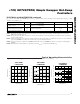
PARAMETER
SYM B O L
C O ND IT IO N S
M IN
T YP
M A X
U N IT S
Supply Voltage
V
S
972V
Supply Current
I
GND
M easur ed out of G N D , P GO O D or PGOOD
op en ci r cui t, D RAIN = V
S
12mA
V
S
= +36V to +72V
91011
External Gate Drive
V
GS
V
S
- V
GATE
V
S
= +9V
8 8.5
V
V
S
= +36V to +72V
5918
Load Voltage Slew-Rate
Magnitude
SR
| dV
DRAIN
/dt |
C
L
= 10µF
V
S
= +9V
3611
V/ms
Default Undervoltage Lockout
V
UVLO
V
S
increasing
28.5 31.5 34.5
V
Undervoltage Lockout
Hysteresis
3.5 V
ON/OFF Pin Input Resistance
R
ON/OFF
19 32 52 kΩ
DRAIN to GND Resistance
R
DGND
900
kΩ
DRAIN to V
S
Resistance R
DS
650
kΩ
ON/OFF Reference Threshold
V
ON/OFF
V
ON/OFF
Increasing
1.14 1.26 1.38
V
ON/OFF Hysteresis
140
mV
Start Delay (Note 3)
t
ON
80
150 280
ms
ON/OFF Off Delay (Note 4)
t
OFF
V
S
- V
GATE
< 1V
51018ms
MAX590_ _AEUT
200 300 460
MAX590_ _BEUT
280 400 540
Circuit-Breaker Threshold
V
CB
V
S
- V
DRAIN
MAX590_ _CEUT
400 500 660
mV
C
GATE
= 1nF
2 6.5
C
GATE
= 4.7nF
411
Circuit-Breaker Delay (Note 5)
t
CB
(V
S
- V
DRAIN
) > V
CB
until (V
S
- V
GATE
)
< 1V, 200mV
overdrive step
C
GATE
= 10nF
717
µs
Restart Delay (Note 3)
t
RS
After circuit breaker event,
MAX590_ A_EUT only
80
150 280
ms
P ow er - G ood O utp ut Low V ol tag e
V
OL
I
OL
= 1mA
0.3 0.6 V