
Datasheet


MAX5895
sources directly to the device without external resistors
to define the DC level. The input resistance of CLKP
and CLKN is 5kΩ.
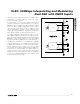
A convenient way to apply a differential signal is with a
balun transformer as shown in Figure 15. Alternatively,
these inputs may be driven from a CMOS-compatible
clock source, however it is recommended to use
sine-wave or AC-coupled differential ECL/PECL drive for
best dynamic performance.
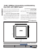
Output Interface (OUTI, OUTQ)
The MAX5895 outputs complementary currents (OUTIP,
OUTIN) and (OUTQP, OUTQN), that can be utilized in a
differential configuration. Load resistors convert these
two output currents into a differential output voltage.
The differential output between OUTIP (OUTQP) and
OUTIN (OUTQN) can be converted to a single-ended
output using a transformer or a differential amplifier.
Figure 16 shows a typical transformer-based applica-
tion circuit for generation of IF output signals. In this
configuration, the MAX5895 operates in differential
mode, which reduces even-order harmonics, and
increases the available output power. Pay close atten-
tion to the transformer core saturation characteristics
when selecting a transformer. Transformer core satura-
tion can introduce strong second harmonic distortion,
16-Bit, 500Msps Interpolating and Modulating
Dual DAC with CMOS Inputs
26 ______________________________________________________________________________________
Figure 15. Single-Ended-to-Differential Clock Conversion Using
a Balun Transformer
SINGLE-ENDED
IINPUT
1:1 RATIO
MINI-CIRCUITS
ADTL1-12
24.9Ω
24.9Ω
CLKP
CLKN
100nF
100nF
MAX5895
Figure 16. Differential-to-Single-Ended Conversion Using Wideband RF Transformers
MAX5895
OUTQP
OUTQN
QDAC
16
1:1
1:1
50Ω
100Ω
50Ω
V
QOUT
, SINGLE-ENDED
OUTIP
OUTIN
IDAC
16
1:1
1:1
50Ω
100Ω
50Ω
V
IOUT
, SINGLE-ENDED