
Datasheet


MAX5895
tionship and detects if the phase drifts more than ±1
data clock cycle. If this occurs, the synchronizer auto-
matically reestablishes synchronization. However, dur-
ing the resynchronization phase, up to 8 data words
may be lost or repeated.
Bit 2 of register 02h disables or enables (default) the
automatic data clock phase detection. Disabling the
data synchronization circuitry requires the data clock
and the DAC clock phase to be locked.
DATACLK Modes
The MAX5895 has a main DATACLK available at
pin 14. An alternate DATACLK is available at pin 27
(DATACLK/B14) when configured in single-port data
input mode (bit 5, address 02h). The DATACLK can be
configured to accept an input clock signal for latching
the input data, or to source a clock signal that can drive
up to 10pF load while latching the input data (bit 3,
address 02h). If DATACLK is configured as an output, it
is frequency divided from the CLKP/CLKN input,
depending on the operating mode, see Table 4.
16-Bit, 500Msps Interpolating and Modulating
Dual DAC with CMOS Inputs
18 ______________________________________________________________________________________
INPUT
MODE
INTERPOLATION
RATE
f
DATA
:f
CLK
f
DAC
:f
CLK
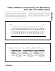
1x 1:1 1:2
2x 1:1 1:1
4x 1:2 1:1
Single
Port
8x 1:4 1:1
1x 1:1 1:1
2x 1:2 1:1
4x 1:4 1:1
Dual Port
8x 1:8 1:1
Table 4. Clock Frequency Ratios in
Various Modes
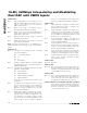
Figure 4. Data Input Timing Diagram
t
D
t
DS
t
CLK
CLKP–CLKN
DATACLK
A0–A15/B0–B15
t
DH