
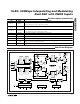
Datasheet


When writing to the MAX5895, data is shifted into SDI;
data is shifted out of SDO in a read operation. Bits 0 to
3 of the control byte are the address bits. These bits set
the address of the register to be written to or read from.
Bits 4 to 6 of the control byte must always be set to 0.
Bit 7 is a read/write bit: 0 for write operation and 1 for
read operation. The most significant bit (MSB) is shifted
in first in default mode. If the serial port is set to LSB-
first mode, both the control byte and data byte are shifted
LSB in first. Figures 1 and 2 show the SPI serial interface
operation in the default write and read mode, respectively.
Figure 3 is a timing diagram for the SPI serial interface.
MAX5895
16-Bit, 500Msps Interpolating and Modulating
Dual DAC with CMOS Inputs
______________________________________________________________________________________ 13
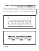
Figure 1. SPI Serial Interface Write Cycle, MSB-First Mode
CS
SCLK
SDI
SDO
10003210
HIGH
IMPEDANCE
IGNORED
ADDRESS DATA
READ CYCLE N - 1
DATA N - 2
10003210
HIGH
IMPEDANCE
IGNORED
ADDRESS DATA
READ CYCLE N
DATA N - 1
10003210
HIGH
IMPEDANCE
IGNORED
ADDRESS DATA
READ CYCLE N + 1
DATA N
0 0 0 0 A3 A2 A1 A0 D7 D6 D5 D4 D3 D2 D1 D0
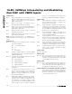
CS
SCLK
SDI
SDO
HIGH IMPEDANCE
Figure 2. SPI Serial Interface Read Cycle, MSB-First Mode