
Datasheet


MAX5894
14-Bit, 500Msps, Interpolating and Modulating
Dual DAC with CMOS Inputs
2 _______________________________________________________________________________________
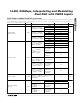
ABSOLUTE MAXIMUM RATINGS
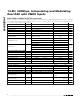
ELECTRICAL CHARACTERISTICS
(DV
DD1.8
= AV
DD1.8
= 1.8V, AV
CLK
= AV
DD3.3
= DV
DD3.3
= 3.3V, modulator off, 2x interpolation, DATACLK output mode, dual-port
mode, 50Ω double-terminated outputs, external reference at 1.25V, T
A
= -40°C to +85°C, unless otherwise noted. Typical values are
at T
A
= +25°C, unless otherwise noted.) (Note 2)
Stresses beyond those listed under “Absolute Maximum Ratings” may cause permanent damage to the device. These are stress ratings only, and functional
operation of the device at these or any other conditions beyond those indicated in the operational sections of the specifications is not implied. Exposure to
absolute maximum rating conditions for extended periods may affect device reliability.
DV
DD1.8
, AV
DD1.8
to GND, DACREF ..................-0.3V to +2.16V
AV
DD3.3
, AV
CLK
, DV
DD3.3
to GND, DACREF........-0.3V to +3.9V
DATACLK, A0–A13, B0–B11,
SELIQ/B13, DATACLK/B12, CS, RESET, SCLK,
DIN and DOUT to GND, DACREF ...-0.3V to (DV
DD3.3
+ 0.3V)
CLKP, CLKN to GND, DACREF..............-0.3V to (AV
CLK
+ 0.3V)
REFIO, FSADJ to GND, DACREF ........-0.3V to (AV
DD3.3
+ 0.3V)
OUTIP, OUTIN, OUTQP,
OUTQN to GND, DACREF..................-1V to (AV
DD3.3
+ 0.3V)
DOUT, DATACLK, DATACLK/B12 Continuous Current........8mA
Continuous Power Dissipation (T
A
= +70°C)
68-Pin QFN (derate 41.7mW/°C above +70°C)
(Note 1) ...................................................................3333.3mW
Junction Temperature......................................................+150°C
Operating Temperature Range ...........................-40°C to +85°C
Storage Temperature Range .............................-65°C to +150°C
Lead Temperature (soldering, 10s) .................................+300°C
Thermal Resistance θ
JC
(Note 1)....................................0.8°C/W
PARAMETER SYMBOL CONDITIONS MIN TYP MAX UNITS
STATIC PERFORMANCE
Resolution 14 Bits
Differential Nonlinearity DNL ±0.5 LSB
Integral Nonlinearity INL ±1.0 LSB
Offset Error OS -0.025 0.003 +0.025 %FS
Offset Drift ±0.03 ppm/°C
Full-Scale Gain Error GE
FS
-4 -0.6 +4 %FS
Gain-Error Drift ±110 ppm/°C
Full-Scale Output Current I
OUTFS
220mA
Output Compliance -0.5 +1.1 V
Output Resistance R
OUT
1MΩ
Output Capacitance C
OUT
5pF
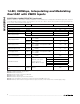
DYNAMIC PERFORMANCE
Maximum Clock Frequency f
CLK
500 MHz
Minimum Clock Frequency f
CLK
1 MHz
Maximum DAC Update Rate f
DAC
f
DAC
= f
CLK
or f
DAC
= f
CLK
/2 500 Msps
Minimum DAC Update Rate f
DAC
f
DAC
= f
CLK
or f
DAC
= f
CLK
/2 1 Msps
Maximum Input Data Rate f
DATA
125 MWps
No interpolation -154
2x interpolation -154
f
DATACLK
= 125MHz,
f
OUT
= 16MHz, f
OFFSET
= 10MHz, -12dBFS
4x interpolation -154
Noise Spectral Density
f
DATACLK
= 125MHz,
f
OUT
= 16MHz, f
OFFSET
= 10MHz, 0dBFS
4x interpolation -151
dBFS/
Hz
Note 1: Thermal resistance based on a multilayer board with 4 x 4 via array in exposed pad area.