
Datasheet


MAX5894
14-Bit, 500Msps, Interpolating and Modulating
Dual DAC with CMOS Inputs
10 ______________________________________________________________________________________
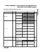
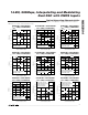
Pin Description
PIN NAME FUNCTION
1 CLKP Noninverting Differential Clock Input. Internally biased to AV
CLK
/2.
2 CLKN Inverting Differential Clock Input. Internally biased to AV
CLK
/2.
3, 4, 5, 24, 25,
42, 43
N.C. Internally Connected. Do not connect.
6, 21, 30, 37 DV
DD1.8
Digital Power Supply. Accepts a 1.71V to 1.89V supply range. Bypass each pin to ground with a
0.1µF capacitor as close to the pin as possible.
7–12, 15–20,
22, 23
A13–A0
A-Port Data Inputs.
Dual-port mode:
I-channel data input. Data is latched on the rising/falling edge (programmable) of the DATACLK.
Single-port mode:
I-channel and Q-channel data input, with SELIQ.
13, 44 DV
DD3.3
CMOS I/O Power Supply. Accepts a 3.0V to 3.6V supply range. Bypass each pin to ground with a
0.1µF capacitor as close to the pin as possible.
14 DATACLK Programmable Data Clock Input/Output. See the DATACLK Modes section for details.
26 SELIQ/B13
Select I-/Q-Channel Input or B-Port MSB Input.
Single-port mode:
If SELIQ = LOW, data is latched into Q-channel on the rising/falling edge (programmable) of
the DATACLK.
If SELIQ = HIGH, data is latched into I-channel on the rising/falling edge (programmable) of the
DATACLK.
Dual-port mode:
Q-channel MSB input.
27 DATACLK/B12
Alternate DATACLK Input/Output or B-Port Bit 12 Input.
Single-port mode:
See the DATACLK Modes section for details.
Dual-port mode:
Q-channel bit 12 input.
If unused connect to GND.
28, 29, 31–36,
38–41
B11–B0
B-Port Data Bits 11–0.
Dual-port mode:
Q-channel inputs. Data is latched on the rising/falling (programmable) edge of the DATACLK.
Single-port mode:
Connect to GND.
45 DOUT Serial-Port Data Output
46 DIN Serial-Port Data Input
47 SCLK Serial-Port Clock Input. Data on DIN is latched on the rising edge of SCLK.
48 CS Serial-Port Interface Select. Drive CS low to enable serial-port interface.
49 RESET Reset Input. Set RESET low during power-up.
50 REFIO Reference Input/Output. Bypass to ground with a 1µF capacitor as close to the pin as possible.
51 DACREF
C ur r ent- S et Resi stor Retur n P ath. For a 20m A ful l - scal e outp ut cur r ent, connect a 2kΩ r esi stor b etw een
FS AD J and D AC RE F. Inter nal l y connected to GN D . D O NO T U SE A S A N EXT ER N A L G R O U N D
C O N N EC T IO N .
52 FSADJ
Full-Scale Adjust Input. This input sets the full-scale output current of the DAC. For a 20mA full-
scale output current, connect a 2kΩ resistor between FSADJ and DACREF.