
Datasheet


MAX5891
16-Bit, 600Msps, High-Dynamic-Performance
DAC with LVDS Inputs
_______________________________________________________________________________________ 5
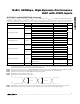
Note 2: Parameter tested with input data pattern based on 16,384 data points. f
OUT
has been chosen so the corresponding input pattern
contains prime number of f
OUT
cycles and is a nonrepetitive sequence. f
OUT
has been rounded to the nearest MHz number in both
the Electrical Characteristics table and Typical Operating Characteristics.
Note 3: Parameter tested exactly at f
OUT
= 16.204833984375MHz and with a clock frequency of 500MHz at an output amplitude of 0dBFS.
Note 4: This parameter does not include update-rate-dependent effects of sin(x)/x filtering inherent in the MAX5891.
Note 5: Parameter measured single-ended with 50Ω double-terminated outputs.
Note 6: Not production tested. Guaranteed by design.
Note 7: Differential input voltage defined as V
D_P
- V
D_N
.
Note 8: Combination of logic-high/-low and common-mode voltages must not exceed absolute maximum rating for D_P/D_N inputs.
Note 9: Parameter defined as the change in midscale output caused by a ±5% variation in the nominal supply voltages.
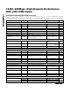
PARAMETER
SYMBOL
CONDITIONS
MIN
TYP
MAX
UNITS
DV
DD3.3
3.135
3.3
3.465
Digital Supply Voltage Range
DV
DD1.8
1.710
1.8
1.890
V
f
CLK
= 100MHz, f
OUT
= 16MHz
26.5
f
CLK
= 500MHz, f
OUT
= 16MHz
26.5 28.5
I
AVDD3.3
f
CLK
= 600MHz, f
OUT
= 16MHz
26.5
f
CLK
= 100MHz, f
OUT
= 16MHz
11.3
f
CLK
= 500MHz, f
OUT
= 16MHz 50 58
Analog Supply Current
I
AVDD1.8
f
CLK
= 600MHz, f
OUT
= 16MHz 61
mA
f
CLK
= 100MHz, f
OUT
= 16MHz 2.8
f
CLK
= 500MHz, f
OUT
= 16MHz 2.8 3.6
Clock Supply Current I
AVCLK
f
CLK
= 600MHz, f
OUT
= 16MHz 2.8
mA
f
CLK
= 100MHz, f
OUT
= 16MHz 0.2
f
CLK
= 500MHz, f
OUT
= 16MHz 0.2 0.5
I
DVDD3.3
f
CLK
= 600MHz, f
OUT
= 16MHz 0.2
f
CLK
= 100MHz, f
OUT
= 16MHz
10.6
f
CLK
= 500MHz, f
OUT
= 16MHz 44 50
Digital Supply Current
I
DVDD1.8
f
CLK
= 600MHz, f
OUT
= 16MHz
50.5
mA
f
CLK
= 100MHz, f
OUT
= 16MHz
137
f
CLK
= 500MHz, f
OUT
= 16MHz
267
301
f
CLK
= 600MHz, f
OUT
= 16MHz
298
mW
Total Power Dissipation P
DISS
Power-down, clock static low,
data input static
13 µW
Power-Supply Rejection Ratio PSRR (Note 9)
±0.025 %FS
ELECTRICAL CHARACTERISTICS (continued)
(AV
DD3.3
= DV
DD3.3
= AV
CLK
= 3.3V, AV
DD1.8
= DV
DD1.8
= 1.8V, external reference V
REFIO
= 1.2V, output load 50Ω double-terminated,
transformer-coupled output, I
OUT
= 20mA, T
A
= -40°C to +85°C, unless otherwise noted. Specifications at T
A
≥ +25°C are guaranteed
by production testing. Specifications at T
A
< +25°C are guaranteed by design and characterization. Typical values are at T
A
= +25°C.)
V
D_N
V
D_P
V
IHLVDS
V
ILLVDS