
Datasheet


MAX5891
16-Bit, 600Msps, High-Dynamic-Performance
DAC with LVDS Inputs
2 _______________________________________________________________________________________
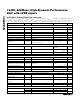
ABSOLUTE MAXIMUM RATINGS
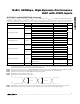
ELECTRICAL CHARACTERISTICS
(AV
DD3.3
= DV
DD3.3
= AV
CLK
= 3.3V, AV
DD1.8
= DV
DD1.8
= 1.8V, external reference V
REFIO
= 1.2V, output load 50Ω double-terminated,
transformer-coupled output, I
OUT
= 20mA, T
A
= -40°C to +85°C, unless otherwise noted. Specifications at T
A
≥ +25°C are guaranteed
by production testing. Specifications at T
A
< +25°C are guaranteed by design and characterization. Typical values are at T
A
= +25°C.)
Stresses beyond those listed under “Absolute Maximum Ratings” may cause permanent damage to the device. These are stress ratings only, and functional
operation of the device at these or any other conditions beyond those indicated in the operational sections of the specifications is not implied. Exposure to
absolute maximum rating conditions for extended periods may affect device reliability.
AV
DD1.8
, DV
DD1.8
to AGND, DGND, DACREF,
and CGND.......................................................-0.3V to +2.16V
AV
DD3.3
, DV
DD3.3
, AV
CLK
to AGND, DGND,
DACREF, and CGND.........................................-0.3V to +3.9V
REFIO, FSADJ to AGND, DACREF,
DGND, and CGND ..........................-0.3V to (AV
DD3.3
+ 0.3V)
OUTP, OUTN to AGND, DGND, DACREF,
and CGND .......................................-1.2V to (AV
DD3.3
+ 0.3V)
CLKP, CLKN to AGND, DGND, DACREF,
and CGND..........................................-0.3V to (AV
CLK
+ 0.3V)
PD to AGND, DGND, DACREF,
and CGND.......................................-0.3V to (DV
DD3.3
+ 0.3V)
Digital Data Inputs (D0N–D15N, D0P–D15P) to AGND,
DGND, DACREF, and CGND ..........-0.3V to (DV
DD1.8
+ 0.3V)
Continuous Power Dissipation (T
A
= +70°C) (Note 1)
68-Pin QFN-EP (derate 28.6mW/°C above +70°C)....3333mW
Thermal Resistance
θ
JA
(Note 1) ....................................24°C/W
Operating Temperature Range ..........................-40°C to +85°C
Junction Temperature .....................................................+150°C
Storage Temperature Range ............................-60°C to +150°C
Lead Temperature (soldering, 10s) ................................+300°C
PARAMETER
SYMBOL
CONDITIONS
MIN TYP MAX
UNITS
STATIC PERFORMANCE
Resolution 16 Bits
Integral Nonlinearity INL Measured differentially
±3.8
LSB
Differential Nonlinearity DNL Measured differentially
±2.8
LSB
Offset Error OS
-0.02 ±0.001 +0.02
%FS
Full-Scale Gain Error GE
FS
External reference -4 ±1 +4
%FS
Internal reference
±130
Gain-Drift Tempco
External reference
±100
ppm/°C
Full-Scale Output Current I
OUT
220mA
Output Compliance Single-ended
-1.0 +1.1
V
Output Resistance R
OUT
1MΩ
Output Capacitance C
OUT
5pF
Output Leakage Current PD = high, power-down mode ±1µA
DYNAMIC PERFORMANCE
Maximum DAC Update Rate
600
Msps
Minimum DAC Update Rate 1
Msps
f
OUT
= 36MHz
A
FULL-SCALE
= -3.5dBm
-163
Noise Spectral Density N
f
CLK
= 500MHz,
-12dBFS, 20MHz
offset from the
carrier
f
OUT
= 151MHz
A
FULL-SCALE
= -6.4dBm
-155
dBFS/Hz
Note 1: Thermal resistance based on a multilayer board with 4x4 via array in exposed paddle area