
Datasheet


MAX5873
12-Bit, 200Msps, High-Dynamic-Performance,
Dual DAC with CMOS Inputs
______________________________________________________________________________________ 13
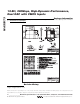
Differential Coupling Using a Wideband RF
Transformer
Use a pair of transformers (Figure 6) or a differential
amplifier configuration to convert the differential voltage
existing between OUTIP/OUTQP and OUTIN/OUTQN to
a single-ended voltage. Optimize the dynamic perfor-
mance by using a differential transformer-coupled out-
put to limit the output power to < 0dBm full scale. Pay
close attention to the transformer core saturation char-
acteristics when selecting a transformer for the
MAX5873. Transformer core saturation can introduce
strong 2nd-order harmonic distortion especially at low
output frequencies and high signal amplitudes. For best
results, center tap the transformer to ground. When not
using a transformer, terminate each DAC output to
ground with a 25Ω resistor. Additionally, place a 50Ω
resistor between the outputs (Figure 7).
For a single-ended unipolar output, select OUTIP
(OUTQP) as the output and ground OUTIN (OUTQN) to
GND. Driving the MAX5873 single-ended is not recom-
mended since additional noise and distortion will
be added.
The distortion performance of the DAC depends on the
load impedance. The MAX5873 is optimized for 50Ω
differential double termination. It can be used with a
transformer output as shown in Figure 6 or just one 25Ω
resistor from each output to ground and one 50Ω resis-
tor between the outputs (Figure 7). This produces a full-
scale output power of up to -2dBm, depending on the
output current setting. Higher termination impedance
can be used at the cost of degraded distortion perfor-
mance and increased output noise voltage.
Grounding, Bypassing, and Power-
Supply Considerations
Grounding and power-supply decoupling can strongly
influence the MAX5873 performance. Unwanted digital
crosstalk couples through the input, reference, power
supply, and ground connections, and affects dynamic
performance. High-speed, high-frequency applications
require closely followed proper grounding and power-
supply decoupling. These techniques reduce EMI and
internal crosstalk that can significantly affect the
MAX5873 dynamic performance.
Use a multilayer PCB with separate ground and power-
supply planes. Run high-speed signals on lines directly
above the ground plane. Keep digital signals as far
away from sensitive analog inputs and outputs, refer-
ence input sense lines, common-mode input, and clock
inputs as practical. Use a symmetric design of clock
input and the analog output lines to minimize 2nd-order
harmonic distortion components, thus optimizing the
DAC’s dynamic performance. Keep digital signal paths
short and run lengths matched to avoid propagation
delay and data skew mismatches.
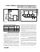
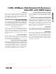
WIDEBAND RF TRANSFORMER
PERFORMS SINGLE-ENDED-TO-
DIFFERENTIAL CONVERSION
SINGLE-ENDED
CLOCK SOURCE
GND
1:1
25Ω
25Ω
CLKP
CLKN
TO DAC
0.1µF
0.1µF
Figure 5. Differential Clock-Signal Generation
MAX5873
12
OUTIP/OUTQP
OUTIN/OUTQN
DATA11–DATA0
WIDEBAND RF TRANSFORMER T2 PERFORMS THE
DIFFERENTIAL-TO-SINGLE-ENDED CONVERSION
T1, 1:1
T2, 1:1
GND
50Ω
100Ω
50Ω
V
OUT
, SINGLE-ENDED
Figure 6. Differential-to-Single-Ended Conversion Using a Wideband RF Transformer