
Datasheet


MAX5864
Ultra-Low-Power, High Dynamic-
Performance, 22Msps Analog Front End
22 ___________________________________________________________________________________________________
0
2
1
4
3
7
6
5
000 010001 011 100 101 110
AT STEP
011 (1/2 LSB )
AT STEP
001 (1/4 LSB )
111
DIGITAL INPUT CODE
ANALOG OUTPUT VALUE
0
2
1
4
3
6
5
000 010001 011 100 101
DIFFERENTIAL LINEARITY
ERROR (-1/4 LSB)
DIFFERENTIAL
LINEARITY ERROR (+1/4 LSB)
1 LSB
1 LSB
DIGITAL INPUT CODE
ANALOG OUTPUT VALUE
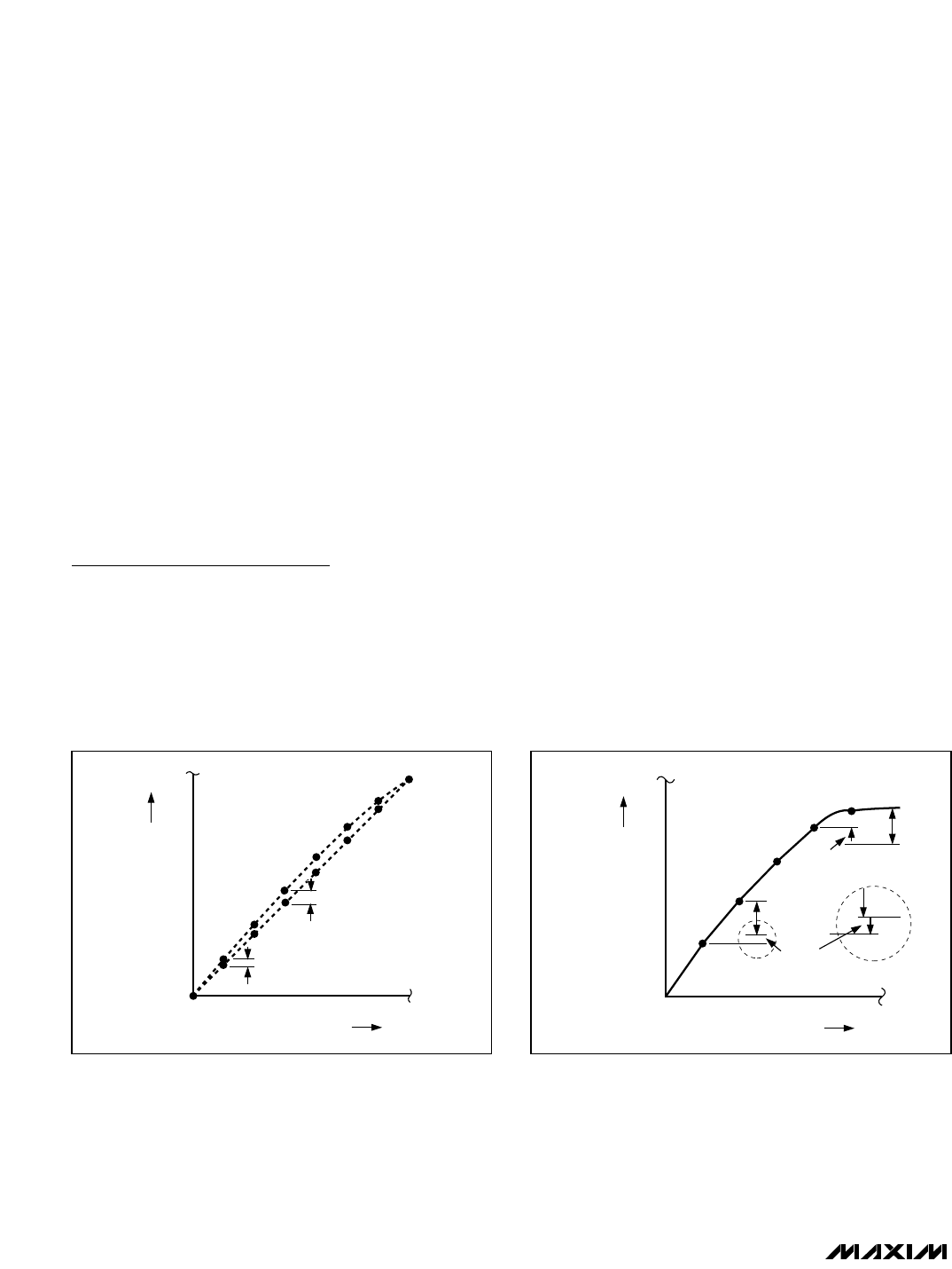
Figure 12a. Integral Nonlinearity Figure 12b. Differential Nonlinearity
Figure 11 illustrates the MAX5864 working with the
MAX2391 and MAX2395 in TDD mode to provide a
complete radio front-end solution. Because the
MAX5864 DAC has full differential analog outputs with
a common-mode level of 1.4V, it can interface directly
with RF quadrature modulators while eliminating dis-
crete components and amplifiers used for level-shifting
circuits. Also, the DAC’s full dynamic range is pre-
served because the internally generated common-
mode level eliminates code-generated level shifting or
attenuation due to resistor level shifting. The MAX5864
ADC has 1V
P-P
full-scale range and accepts input com-
mon-mode levels of V
DD
/2 (±200mV). These features
simplify the analog interface between RF quadrature
demodulator and ADC while eliminating discrete gain
amplifiers and level-shifting components.
Grounding, Bypassing, and
Board Layout
The MAX5864 requires high-speed board layout design
techniques. Refer to the MAX5865 EV kit data sheet for
a board layout reference. Locate all bypass capacitors
as close to the device as possible, preferably on the
same side of the board as the device, using surface-
mount devices for minimum inductance. Bypass V
DD
to
GND with a 0.1µF ceramic capacitor in parallel with a
2.2µF capacitor. Bypass OV
DD
to OGND with a 0.1µF
ceramic capacitor in parallel with a 2.2µF capacitor.
Bypass REFP, REFN, and COM each to GND with a
0.33µF ceramic capacitor. Bypass REFIN to GND with
a 0.1µF capacitor.
Multilayer boards with separated ground and power
planes yield the highest level of signal integrity. Use a
split ground plane arranged to match the physical loca-
tion of the analog ground (GND) and the digital output
driver ground (OGND) on the device package. Connect
the MAX5864 exposed backside paddle to the GND
plane. Join the two ground planes at a single point
such that the noisy digital ground currents do not inter-
fere with the analog ground plane. The ideal location
for this connection can be determined experimentally at
a point along the gap between the two ground planes.
Make this connection with a low-value, surface-mount
resistor (1Ω to 5Ω), a ferrite bead, or a direct short.
Alternatively, all ground pins could share the same
ground plane, if the ground plane is sufficiently isolated
from any noisy digital system’s ground plane (e.g.,
downstream output buffer or DSP ground plane).
Route high-speed digital signal traces away from sensi-
tive analog traces. Make sure to isolate the analog
input lines to each respective converter to minimize
channel-to-channel crosstalk. Keep all signal lines short
and free of 90° turns.