
Datasheet


MAX5864
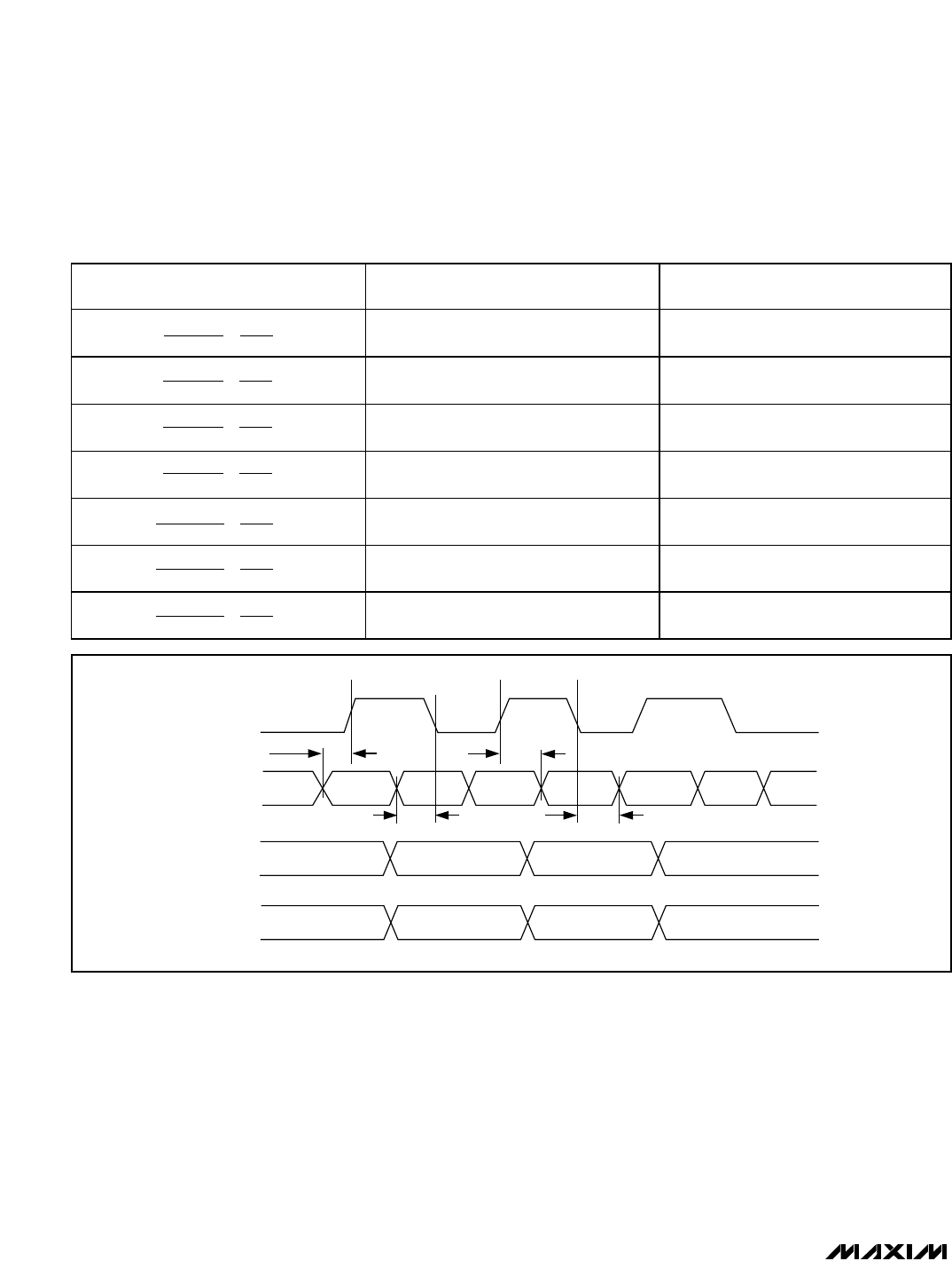
DAC Timing
Figure 4 shows the relationship between the clock, input
data, and analog outputs. Data for the I channel (ID) is
latched on the falling edge of the clock signal, and Q-
channel (QD) data is latched on the rising edge of the
clock signal. Both I and Q outputs are simultaneously
updated on the next rising edge of the clock signal.
3-Wire Serial Interface and
Operation Modes
The 3-wire serial interface controls the MAX5864 opera-
tion modes. Upon power-up, the MAX5864 must be
programmed to operate in the desired mode. Use the
3-wire serial interface to program the device for the shut-
down, idle, standby, Rx, Tx, or Xcvr mode. An 8-bit data
register sets the operation modes as shown in Table 3.
The serial interface remains active in all six modes.
Ultra-Low-Power, High Dynamic-
Performance, 22Msps Analog Front End
16 ______________________________________________________________________________________
Table 2. DAC Output Voltage vs. Input Codes (Internal Reference Mode V
REFDAC
=
1.024V, External Reference Mode V
REFDAC
= V
REFIN
)
DIFFERENTIAL OUTPUT VOLTAGE
OFFSET BINARY
(DD0–DD9)
INPUT DECIMAL CODE
11 1111 1111 1023
11 1111 1110 1022
10 0000 0001 513
10 0000 0000 512
01 1111 1111 511
00 0000 0001 1
00 0000 0000 0
V
REFDAC
2.56
1023
1023
×
V
REFDAC
2.56
1021
1023
×
V
REFDAC
2.56
3
1023
×
V
REFDAC
2.56
1
1023
×
V
REFDAC
2.56
1
1023
×
−
V
REFDAC
2.56
1021
1023
×
−
V
REFDAC
2.56
1023
1023
×
−
Figure 4. DAC System Timing Diagram
t
DSQ
t
DSI
Q: N-2 I: N-1
DD0–DD9
CLK
ID
QD
Q: N-1
I: N
Q: N I: N+1
N-2
N-1
N
N-2
N-1
N
t
DHQ
t
DHI