
Datasheet


MAX5823/MAX5824/MAX5825
Ultra-Small, Octal Channel, 8-/10-/12-Bit Buffered
Output DACs with Internal Reference and I
2
C Interface
7Maxim Integrated
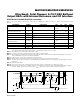
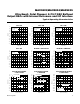
Figure 1. I
2
C Serial Interface Timing Diagram
ELECTRICAL CHARACTERISTICS (continued)
(V
DD
= 2.7V to 5.5V, V
DDIO
= 1.8V to 5.5V, V
GND
= 0V, C
L
= 200pF, R
L
= 2kI, T
A
= -40NC to +125NC, unless otherwise noted.)
(Note 3)
Note 3: Electrical specifications are production tested at T
A
= +25°C. Specifications over the entire operating temperature range
are guaranteed by design and characterization. Typical specifications are at T
A
= +25°C.
Note 4: DC performance is tested without load, V
REF
= V
DD
.
Note 5: Linearity is tested with unloaded outputs to within 20mV of GND and V
DD
.
Note 6: Offset and gain calculated from measurements made with V
REF
= V
DD
at code 30 and 4065 for MAX5825, code 8 and
1016 for MAX5824, and code 2 and 254 for MAX5823.
Note 7: Subject to zero- and full-scale error limits and V
REF
settings.
Note 8: Measured with all other DAC outputs at midscale with one channel transitioning 0 to full scale.
Note 9: On power-up, the device initiates an internal 200µs (typ) calibration sequence. All commands issued during this time will
be ignored.
Note 10: Guaranteed by design.
Note 11: All channels active at V
FS
, unloaded. Static logic inputs with V
IL
= V
GND
and V
IH
= V
DDIO
for all inputs .
Note 12: Unconnected conditions on the ADDR_ inputs are sensed through a resistive pullup and pulldown operation; for proper
operation, ADDR_ inputs must be connected to V
DDIO
, GND, or left unconnected with minimal capacitance.
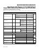
PARAMETER SYMBOL CONDITIONS MIN TYP MAX UNITS
SDA and SCL Receiving Fall
Time
t
F
20 +
C
B
/10
300 ns
SDA Transmitting Fall Time t
F
20 +
C
B
/10
250 ns
Setup Time for STOP Condition t
SU;STO
0.6 Fs
Bus Capacitance Allowed C
B
V
DD
= 2.7V to 5.5V 10 400 pF
Pulse Width of Suppressed Spike t
SP
50 ns
CLR Removal Time Prior to a
Recognized START
t
CLRSTA
100 ns
CLR Pulse Width Low t
CLPW
20 ns
LDAC Pulse Width Low t
LDPW
20 ns
LDAC Fall to SCLK Rise Hold t
LDH
400 ns
t
SU;STO
t
R
t
SP
t
HD;STA
t
SU;STA
t
F
t
HIGH
t
HD;DAT
t
LOW
t
CLPW
t
CLRSTA
t
LDH
t
LDPW
t
HD;STA
t
F
SS
S
r
P
SDA
SCL
CLR
LDAC
t
SU;DAT
t
F
t
BUF