
Datasheet


MAX5823/MAX5824/MAX5825
Ultra-Small, Octal Channel, 8-/10-/12-Bit Buffered
Output DACs with Internal Reference and I
2
C Interface
20Maxim Integrated
Readback of individual RETURN registers is supported
for RETURN commands (B[23:20] = 0111). For this com-
mand, which supports a DAC address, the requested
channel RETURN register content will be returned,
along with the selected DAC address. If all DACs are
selected, readback will begin with RETURN0 content
and will progress through the remaining DAC channels.
The RETURN_ALL (B[23:16] = 11000011) command
behaves identically to the RETURN command with all
DACs selected.
Readback of individual CODE registers is supported for
the CODE commands (B[23:20] = 1000). For this com-
mand, which supports a DAC address, the requested
channel CODE register content will be returned, along
with the selected DAC address. If all DACs are select-
ed, readback will begin with CODE0 content and will
progress through the remaining DAC channels. The
CODE_ALL (B[23:16] = 11000000) command behaves
identically to the CODE command with all DACs selected.
Readback of individual DAC registers is supported for
all LOAD commands (B[23:20] = 1001, 1010, 1011). For
these commands, which support a DAC address, the
requested DAC register content will be returned, along
with the selected DAC address. If all DACs are selected,
readback will begin with DAC0 content and will progress
through the remaining DAC channels. The LOAD_ALL
and CODE_ALL_LOAD_ALL commands (B[23:16] =
11000001 and 11000010, respectively) behave identi-
cally to the LOAD command with all DACs selected.
Modified readback of the POWER register is supported
for the POWER command (B[23:20] = 0100). The power
status of each DAC is reported in locations B[7:0], with a
1 indicating the DAC is powered down and a zero indi-
cating the DAC is operational (see Table 2).
Readback of all other registers is not directly supported.
All requests to read unsupported registers reads back
the device’s current watchdog timer status (WD:0 = nor-
mal, 1 = timed out), reference setting (REF[2:0]), and CLR
condition, along with the device revision (B[10:8] = 001)
and part ID (B[7:0]) in the format as shown in Table 2.
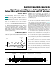
Interface Verification I
2
C
Readback Operations
While the MAX5823/MAX5824/MAX5825 support stan-
dard I
2
C readback of selected registers, it is also
capable of functioning in an interface verification mode.
This mode is accessed any time a readback operation
follows an executed write mode command. In this mode,
the last executed three-byte command is read back in its
entirety. This behavior allows verification of the interface.
Sample command sequences are shown in Figure 7.
The first command transfer is given in write mode with
R/W = 0 and must be run to completion to qualify for
interface verification readback. There is now a STOP/
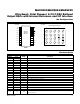
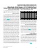
Table 2. Standard I
2
C User Readback Data
COMMAND BYTE (REQUEST) READBACK DATA HIGH BYTE READBACK DATA LOW BYTE
B23 B22 B21 B20 B19 B18 B17 B16 B15 B14 B13 B12 B11 B10 B9 B8 B7 B6 B5 B4 B3 B2 B1 B0
0 0 0 1 X X X X WDOG Timeout Selection[11:4] Timeout Selection[3:0] WDM WL[1:0] 0
0 1 0 0 X X X X 0 0 0 0 0 0 0 0 PW7 PW6 PW5 PW4 PW3 PW2 PW1 PW0
0 1 1 1 DAC SELECTION RETURNn[11:4] RETURNn[3:0] ADDRESSn[3:0]
1 0 0 0 DAC SELECTION CODEn[11:4] CODEn[3:0] ADDRESSn[3:0]
1 0 0 1 DAC SELECTION DACn[11:4] DACn[3:0] ADDRESSn[3:0]
1 0 1 0 DAC SELECTION DACn[11:4] DACn[3:0] ADDRESSn[3:0]
1 0 1 1 DAC SELECTION DACn[11:4] DACn[3:0] ADDRESSn[3:0]
1 1 0 0 0 0 0 0 CODE0[11:4] CODE0[3:0] ADDRESS0[3:0]
1 1 0 0 0 0 0 1 DAC0[11:4] DAC0[3:0] ADDRESS0[3:0]
1 1 0 0 0 0 1 0 DAC0[11:4] DAC0[3:0] ADDRESS0[3:0]
1 1 0 0 0 0 1 1 RETURN0[11:4] RETURN0[03:0] ADDRESS0[3:0]
All Other Commands (MAX5825)
WD REF[2:0]
CLR
REV_ID
[2:0]
(001)
1 0 0 0 0 0 0 0
All Other Commands (MAX5824) 1 0 1 0 0 0 0 0
All Other Commands (MAX5823) 1 0 0 1 0 0 0 0