
Datasheet


MAX5823/MAX5824/MAX5825
Ultra-Small, Octal Channel, 8-/10-/12-Bit Buffered
Output DACs with Internal Reference and I
2
C Interface
18Maxim Integrated
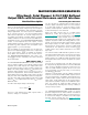
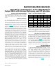
Figure 3. I
2
C Acknowledge
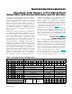
Figure 4. I
2
C Single Register Write Sequence
I
2
C Slave Address
The slave address is defined as the seven most sig-
nificant bits (MSBs) followed by the R/W bit. See
Figure 4. The three most significant bits are 001 with the
4 LSBs determined by ADDR1 and ADDR0 as shown in
Table 1. Setting the R/W bit to 1 configures the MAX5823/
MAX5824/MAX5825 for read mode. Setting the R/W bit to
0 configures the MAX5823/MAX5824/MAX5825 for write
mode. The slave address is the first byte of informa-
tion sent to the MAX5823/MAX5824/MAX5825 after the
START condition.
The MAX5823/MAX5824/MAX5825 has the ability to
detect an unconnected (N.C.) state on the ADDR_ inputs
for additional address flexibility; if disconnecting the
ADDR_ inputs, be certain to minimize all loading on the
ADDR_ inputs (i.e. provide a landing for ADDR_, but do
not allow any board traces).
I
2
C Broadcast Address
A broadcast address is provided for the purpose of
updating or configuring all MAX5823/MAX5824/MAX5825
devices on a given I
2
C bus. All MAX5823/MAX5824/
MAX5825 devices acknowledge and respond to the
broadcast device address 00101000, regardless of the
state of the address pins. The broadcast mode is intend-
ed for use in write mode only (as indicated by R/W = 0 in
the address given).
I
2
C Acknowledge
In write mode, the acknowledge bit (ACK) is a clocked 9th
bit that the MAX5823/MAX5824/MAX5825 use to hand-
shake receipt of each byte of data as shown in Figure 3.
The MAX5823/MAX5824/MAX5825 pull down SDA during
the entire master-generated 9th clock pulse if the previous
byte is successfully received. Monitoring ACK allows for
detection of unsuccessful data transfers. An unsuccessful
data transfer occurs if a receiving device is busy or if a
system fault has occurred. In the event of an unsuccess-
ful data transfer, the bus master will retry communication.
In read mode, the master pulls down SDA during the
9th clock cycle to acknowledge receipt of data from the
MAX5823/MAX5824/MAX5825. An acknowledge is sent
by the master after each read byte to allow data transfer
to continue. A not-acknowledge is sent when the master
reads the final byte of data from the MAX5823/MAX5824/
MAX5825, followed by a STOP condition.
I
2
C Command Byte and Data Bytes
A command byte follows the slave address. A command
byte is typically followed by two data bytes unless it is
the last byte in the transmission. If data bytes follow the
command byte, the command byte indicates the address
of the register that is to receive the following two data
bytes. The data bytes are stored in a temporary register
and then transferred to the appropriate register during
the ACK periods between bytes. This avoids any glitch-
ing or digital feedthrough to the DACs while the interface
is active.
1
SCL
START
CONDITION
SDA
29
CLOCK PULSE
FOR
ACKNOWLEDGMENT
ACKNOWLEDGE
NOT ACKNOWLEDGE
SCL
A 20 19 18 17 A16 15 14 13 12 11 10 9A8
START
SDA
WRITE ADDRESS
BYTE #1: I
2
C SLAVE ADDRESS
WRITE COMMAND
BYTE #2: COMMAND BYTE
(B[23:16])
WRITE DATA
BYTE #3: DATA HIGH BYTE
(B[15:8])
WRITE DATA
BYTE #4: DATA LOW BYTE
(B[7:0])
212223
STOP
7 6 5 4 3 2 1 A0
ACK. GENERATED BY MAX5823/MAX5824/MAX5825
COMMAND EXECUTED
A3 A2 A1 A0 W100
A