
Datasheet


7Maxim Integrated
MAX5713/MAX5714/MAX5715
Ultra-Small, Quad-Channel, 8-/10-/12-Bit Buffered
Output DACs with Internal Reference and SPI Interface
Note 3: Electrical specifications are production tested at T
A
= +25°C. Specifications over the entire operating temperature range
are guaranteed by design and characterization. Typical specifications are at T
A
= +25°C.
Note 4: DC Performance is tested without load.
Note 5: Linearity is tested with unloaded outputs to within 20mV of GND and V
DD
.
Note 6: Offset and gain errors are calculated from measurements made with V
REF
= V
DD
at code 30 and 4065 for MAX5715,
code 8 and 1016 for MAX5714, and code 2 and 254 for MAX5713.
Note 7: Subject to zero and full-scale error limits and V
REF
settings.
Note 8: Measured with all other DAC outputs at midscale with one channel transitioning 0 to full scale.
Note 9: On power-up, the device initiates an internal 200µs (typ) calibration sequence. All commands issued during this time will
be ignored.
Note 10: Guaranteed by design.
Note 11: All channels active at V
FS
, unloaded. Static logic inputs with V
IL
= V
GND
and V
IH
= V
DDIO
.
Note 12: Daisy-chain speed is relaxed to accommodate (t
CRF
+ t
CSS0
) with margin (derived specification, not production tested).
Note 13: This specification and its propagation through the chain limits how quickly an aborted daisy-chain command can be fol-
lowed by another daisy-chain command, to be applied on a per-device basis.
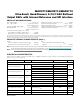
Figure 1. SPI Serial Interface Timing Diagram
ELECTRICAL CHARACTERISTICS (continued)
(V
DD
= 2.7V to 5.5V, V
DDIO
= 1.8V to 5.5V, V
GND
= 0V, C
L
= 200pF, R
L
= 2kI, T
A
= -40NC to +125NC, unless otherwise noted. Typical
values are at T
A
= +25NC.) (Note 3)
PARAMETER SYMBOL CONDITIONS MIN TYP MAX UNITS
SCLK Fall to RDY Fall
t
CRF
Applies to 24th SCLK falling edge,
C
LOAD
= 20pF
40 ns
SCLK Fall to RDY Hold
t
CRH
Applies to 24th SCLK falling edge,
C
LOAD
= 0pF
2 ns
CSB Rise to RDY Rise
t
CSR
C
LOAD
= 20pF (Note 13) 40 ns
D
IN
23 D
IN
22 D
IN
21 D
IN
20 D
IN
19 D
IN
18 D
IN
17 D
IN
16 D
IN
2 D
IN
1
t
CSA
t
CSF
t
LDPW
t
LDH
t
CSH1
D
IN
0 D
IN
23
1SCLK
CSB
DIN
234567822232
41
t
CSH0
t
CSPW
t
CLPW
t
CSC
t
CSS0
t
CH
t
CL
t
DH
t
DS
t
SCLK
LDAC
CLR