
Datasheet


16Maxim Integrated
MAX5713/MAX5714/MAX5715
Ultra-Small, Quad-Channel, 8-/10-/12-Bit Buffered
Output DACs with Internal Reference and SPI Interface
Clear Input (CLR)
The MAX5713/MAX5714/MAX5715 feature an asynchro-
nous active-low CLR logic input that simultaneously sets
all four DAC outputs to zero. Driving CLR low clears the
contents of both the CODE and DAC registers and also
aborts the on-going SPI command. To allow a new SPI
command, drive CLR high, satisfying the t
CSC
timing
requirement.
Interface Power Supply (V
DDIO
)
The MAX5713/MAX5714/MAX5715 feature a separate
supply pin (V
DDIO
) for the digital interface (1.8V to 5.5V).
Connect V
DDIO
to the I/O supply of the host processor.
SPI Serial Interface
The MAX5713/MAX5714/MAX5715 3-wire serial interface
is compatible with MICROWIRE, SPI, QSPI, and DSPs.
The interface provides three inputs, SCLK, CSB, and
DIN. The chip-select input (CSB, active low) frames the
data loaded through the serial data input (DIN). Following
a CSB input high-to-low transition, the data is shifted
in synchronously and latched into the input register on
each falling edge of the serial clock input (SCLK). Each
serial operation word is 24-bits long. The DAC data is
left justified as shown in Table 1. The serial input register
transfers its contents to the destination registers after
loading 24 bits of data on the 24th SCLK falling edge.
To initiate a new SPI operation, drive CSB high and then
low to begin the next operation sequence, being sure to
meet all relevant timing requirements. During CSB high
periods, SCLK is ignored, allowing communication to
other devices on the same bus. SPI operations consist-
ing of more than 24 SCLK cycles are executed on the
24th SCLK falling edge, using the first three bytes of
data available. SPI operations consisting of less than 24
SCLK cycles will not be executed. The content of the SPI
operation consists of a command byte followed by a two
byte data word.
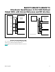
Figure 1 shows the timing diagram for the complete
3-wire serial interface transmission. The DAC code
settings (D) for the MAX5713/MAX5714/MAX5715 are
accepted in an offset binary format (see Table 1).
Otherwise, the expected data format for each command
is listed in Table 2. See Figure 3 for an example of a typi-
cal SPI circuit application.
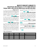
SPI Daisy Chain/RDY Output
(TSSOP Package Only)
The elongated programming operation is typically used
for devices in daisy-chain applications. The RDY out-
put in the TSSOP version of the MAX5713/MAX5714/
MAX5715 feeds the CSB input of the next device in the
daisy-chain. The MAX5713/MAX5714/MAX5715 pulls the
RDY output low on the 24th SCLK falling edge, allowing
the next device in the chain to begin its SPI operation,
commencing with the 25th SCLK falling edge. See Figure
2 for timing characteristics of the elongated SPI program-
ming operation. In practice (t
CRF
+ t
CSS0
) requirements
will limit the daisy-chain SPI speed. Also in daisy-chain
applications, a partial write to the chain is possible
as long as the t
CSA
is met for the first device the user
chooses not to program. See Figure 4 for an example of
a daisy-chain circuit application.
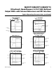
Table 1. Format DAC Data Bit Positions
PART B15 B14 B13 B12 B11 B10 B9 B8 B7 B6 B5 B4 B3 B2 B1 B0
MAX5713 D7 D6 D5 D4 D3 D2 D1 D0 x x x x x x x x
MAX5714 D9 D8 D7 D6 D5 D4 D3 D2 D1 D0 x x x x x x
MAX5715 D11 D10 D9 D8 D7 D6 D5 D4 D3 D2 D1 D0 x x x x