
Datasheet

MAX5712
12-Bit, Low-Power, Rail-to-Rail
Voltage-Output Serial DAC in SOT23
8
Maxim Integrated
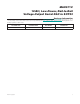
Shutdown Modes
The MAX5712 includes three software-controlled shut-
down modes that reduce the supply current to below
1µA. In two of the three shutdown modes, OUT is con-
nected to GND through a resistor. Table 1 lists the
three shutdown modes of operation.
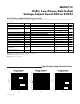
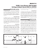
Applications Information
Device Powered by an
External Reference
The MAX5712 generates an output voltage proportional
to V
DD
, coupling power supply noise to the output. The
circuit in Figure 2 rejects this power-supply noise by
powering the device directly with a precision voltage
reference, improving overall system accuracy. The
MAX6030 (+3V, 75ppm) or the MAX6050 (+5V, 75ppm)
precision voltage references are ideal choices due to
the low-power requirements of the MAX5712. This solu-
tion is also useful when the required full-scale output
voltage is less than the available supply voltages.
Digital Inputs and Interface Logic
The 3-wire digital interface for the MAX5712 is compati-
ble with SPI, QSPI, MICROWIRE, and DSP. The three
digital inputs (CS, DIN, and SCLK) load the digital input
serially into the DAC. All of the digital inputs include
Schmitt-trigger buffers to accept slow-transition inter-
faces. This allows optocouplers to interface directly to
the MAX5712 without additional external logic. The digi-
tal inputs are compatible with CMOS-logic levels.
Power-Supply Bypassing and Layout
Careful PC board layout is important for optimal system
performance. Keep analog and digital signals separate
to reduce noise injection and digital feedthrough. Use a
ground plane to ensure that the ground return from
GND to the supply ground is short and low impedance.
Bypass V
DD
with a 0.1µF capacitor to ground as close
as possible to the device.
Chip Information
PROCESS: BiCMOS
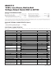
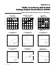
16-BIT SERIAL WORD
MSB LSB MODE OUTPUT
C3 C2 C1 C0 D11 D10 D09 D08 D07 D06 D05 D04 D03 D02 D01 D00
0 0 0 0 12-Bit DAC Code
Set and update
DAC
V
OUT
= V
DD
x
CODE/4096
1 111XXXXXXXXXX00 Wake-Up
Current DAC
setting (initially 0)
1 111XXXXXXXXXX01 Power-Down Floating
1 111XXXXXXXXXX10 Power-Down 1kΩ to GND
1 111XXXXXXXXXX11 Power-Down
100kΩ to GND
Table 1. Serial Interface Mapping
V
DD
GND
OUT
GND
OUT
MAX6050
MAX6030
MAX5712
IN
Figure 2. MAX5712 Powered By Reference
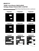
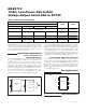
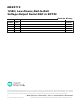
GND
SCLKDIN
1 6 OUT
5
V
DD
MAX5712
SOT23
TOP VIEW
2
34
CS
Pin Configuration