
Datasheet

MAX5712
12-Bit, Low-Power, Rail-to-Rail
Voltage-Output Serial DAC in SOT23
2
Maxim Integrated
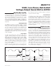
ABSOLUTE MAXIMUM RATINGS
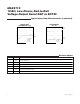
ELECTRICAL CHARACTERISTICS
(V
DD
= +2.7V to +5.5V, GND = 0, R
L
= 5kΩ, C
L
= 200pF, T
A
= T
MIN
to T
MAX
, unless otherwise noted. Typical values are at V
DD
= +5V.
T
A
= +25°C)
Stresses beyond those listed under “Absolute Maximum Ratings” may cause permanent damage to the device. These are stress ratings only, and functional
operation of the device at these or any other conditions beyond those indicated in the operational sections of the specifications is not implied. Exposure to
absolute maximum rating conditions for extended periods may affect device reliability.
V
DD
to GND..............................................................-0.3V to +6V
OUT, SCLK, DIN, CS to GND......................-0.3V to (V
DD
+ 0.3V)
Maximum Current into Any Pin .........................................±50mA
Continuous Power Dissipation (T
A
= +70°C)
6-Pin SOT23 (derate 9.1mW/°C above +70°C)...........727mW
Operating Temperature Range .........................-40°C to +125°C
Maximum Junction Temperature .....................................+150°C
Storage Temperature Range .............................-65°C to +150°C
Lead Temperature (soldering, 10s) .................................+300°C
Soldering Temperature (reflow) .......................................+260°C
PARAMETER SYMBOL CONDITIONS MIN TYP MAX UNITS
STATIC ACCURACY (NOTE 1)
Resolution N 12 Bits
Differential Nonlinearity Error DNL Guaranteed monotonic (Note 2) ±1 LSB
Integral Nonlinearity Error INL (Note 2) ±2 ±16 LSB
Zero-Code Error OE Code = 000 0.4 1.5 % of FS
Zero-Code Error Tempco 2.3 ppm/°C
Gain Error GE Code = FFF hex -3 % of FS
Gain-Error Tempco Integral 0.26 ppm/°C
DAC OUTPUT
Output Voltage Range No-load (Note 3) 0 V
DD
V
DC Output Impedance Code = 800 hex 0.8 Ω
V
DD
= +3V 15
Short Circuit Current
V
DD
= +5V 48
mA
V
DD
= +3V 8
Wake-Up Time
V
DD
= +5V 8
µs
Output Leakage Current Power-down mode = output high-impedance ±18 ±33 nA
DIGITAL INPUTS (SCLK, DIN, CS)
Input High Voltage V
IH
V
DD
= +3V, +5V 0.7 x V
DD
V
Input Low Voltage V
IL
V
DD
= +3V, +5V 0.3 x V
DD
V
Input Leakage Current I
IN
Digital Inputs = 0 or V
DD
±0.1 ±1µA
Input Capacitance C
IN
5pF
DYNAMIC PERFORMANCE
Voltage-Output Slew Rate SR 0.5 V/µs
Voltage-Output Settling Time 400 hex to C00 hex (Note 4) 4 10 µs
Digital Feedthrough Any digital inputs from 0 to V
DD
0.2 nV-s
Digital-Analog Glitch Impulse
Major carry transition (code 7FF hex to code
800 hex)
12 nV-s
PACKAGE THERMAL CHARACTERISTICS (Note 1)
SOT23
Junction-to-Ambient Thermal Resistance (θ
JA
)...............134.40°C/W
Junction-to-Case Thermal Resistance (θ
JC
)......................39°C/W