
Datasheet


MAX5711
10-Bit, Low-Power, Rail-to-Rail
Voltage-Output Serial DAC in SOT23
8 _______________________________________________________________________________________
falling edge of CS. Not keeping CS low during the first
15 SCLK cycles discards input data. The serial clock
(SCLK) can idle either high or low between transitions.
Figure 1 shows the complete 3-wire serial interface
transmission. Table 1 lists serial-interface mapping. The
first command after V
DD
is applied must be the wake-
up command.
Power-Down Modes
The MAX5711 includes three software-controlled
power-down modes that reduce the supply current to
below 1µA. In two of the three power-down modes,
OUT is connected to GND through a resistor. Table 1
lists the three power-down modes of operation. When in
power-down, the MAX5711 does not respond to the
“set and update” command.
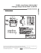
Applications Information
Device Powered by
an External Reference
The MAX5711 generates an output voltage proportional
to V
DD
, coupling power-supply noise to the output. The
circuit in Figure 2 rejects this power-supply noise by
powering the device directly with a precision voltage
reference, improving overall system accuracy. The
MAX6030 (+3V, 75ppm) or the MAX6050 (+5V, 75ppm)
precision voltage references are ideal choices due to
the low-power requirements of the MAX5711. This solu-
tion is also useful when the required full-scale output
voltage is less than the available supply voltages.
Digital Inputs and Interface Logic
The 3-wire digital interface for the MAX5711 is compati-
ble with SPI, QSPI, MICROWIRE, and DSP. The three
digital inputs (CS, DIN, and SCLK) load the digital input
serially into the DAC. All of the digital inputs include
Schmitt-trigger buffers to accept slow-transition inter-
faces. This allows optocouplers to interface directly to
the MAX5711 without additional external logic. The digi-
tal inputs are compatible with CMOS-logic levels.
Power-Supply Bypassing and Layout
Careful PC board layout is important for optimal system
performance. Keep analog and digital signals separate
to reduce noise injection and digital feedthrough. Use a
ground plane to ensure that the ground return from
GND to the supply ground is short and low impedance.
Bypass V
DD
with a 0.1µF capacitor to ground as close
as possible to the device.
Chip Information
TRANSISTOR COUNT: 3856
PROCESS: BiCMOS
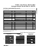
16-BIT SERIAL WORD
MSB
LSB
MODE OUTPUT
C3
C2 C1 C0 D09 D08 D07 D06 D05 D04 D03 D02 D01 D00 S1 S0
0
000
10-Bit DAC Code
00
Set and Update
DAC
V
OUT
= V
DD
x
CODE/1024
1
111XXXXXXXXXX00
Wake-Up
Current DAC
setting (initially 0)
1
111XXXXXXXXXX01
Power-Down Floating
1
111XXXXXXXXXX10
Power-Down 1kΩ to GND
1
111XXXXXXXXXX11
Power-Down
100kΩ to GND
Table 1. Serial Interface Mapping
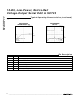
V
DD
GND
OUTIN
GND
OUT
MAX6050
MAX6030
MAX5711
Figure 2. MAX5711 Powered By Reference
X = Don’t Care