
Datasheet

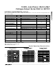


-4
-2
-3
0
-1
1
2
3
4
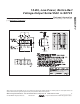
0 256 384128 512 640 768 896 1024
MAX5711 toc01
CODE
INL (LSB)
INTEGRAL NONLINEARITY
vs. CODE (T
A
= +25°C)
V
DD
= +5V
V
DD
= +3V
MAX5711
10-Bit, Low-Power, Rail-to-Rail
Voltage-Output Serial DAC in SOT23
_______________________________________________________________________________________ 3
Note 1: DC specifications are tested without output loads.
Note 2: Linearity guaranteed from code 29 to code 995.
Note 3: Offset and gain error limit the FSR.
Note 4: Guaranteed by design.
ELECTRICAL CHARACTERISTICS (continued)
(V
DD
= +2.7V to +5.5V, GND = 0, R
L
= 5kΩ, C
L
= 200pF, T
A
= T
MIN
to T
MAX
, T
A
= +25°C, unless otherwise noted. Typical values are at
V
DD
= +5V, T
A
= +25°C.)
PARAMETER
SYMBOL
CONDITIONS
MIN TYP MAX
UNITS
DYNAMIC PERFORMANCE
Voltage Output Slew Rate SR 0.5 V/µs
Voltage Output Settling Time 100 hex to 300 hex (Note 4) 4 10 µs
Digital Feedthrough Any digital inputs from 0 or V
DD
0.2 nV-s
Digital-Analog Glitch Impulse
Major carry transition (code 1FF hex to code
200 hex)
12 nV-s
POWER REQUIREMENTS
Supply Voltage Range V
DD
2.7 5.5 V
All digital inputs at 0 or V
DD
, V
DD
= 3.6V 85 150
Supply Current with No Load I
DD
All digital inputs at 0 or V
DD
, V
DD
= 5.5V
105
187
µA
Power-Down Supply Current
I
DDPD
All digital inputs at 0 or V
DD
, V
DD
= 5.5V
0.29
1
µA
TIMING CHARACTERISTICS (FIGURE 2) (Timing is tested with no load)
SCLK Clock Frequency
f
SCLK
020MHz
SCLK Pulse Width High t
CH
20 ns
SCLK Pulse Width Low t
CL
20 ns
CS Fall to SCLK Rise Setup
t
CSS
15 ns
DIN Setup Time t
DS
15 ns
DIN Hold Time t
DH
0ns
SCLK Falling Edge to CS Rising
Edge
t
CSH
10 ns
CS Pulse Width High t
CSW
80 ns
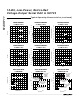
Typical Operating Characteristics
(T
A
= +25°C, unless otherwise noted.)
-0.20
-0.10
-0.15
0
-0.05
0.05
0.10
0.15
0.20
0 256 384128 512 640 768 896 1024
MAX5711 toc02
CODE
DNL (LSB)
DIFFERENTIAL NONLINEARITY
vs. CODE (T
A
= +25°C)
V
DD
= +3V OR +5V
-1.0
-0.6
-0.8
-0.2
-0.4
0.2
0
0.4
0.8
0.6
1.0
0 256 384128 512 640 768 896 1024
MAX5711 toc03
CODE
TOTAL UNADJUSTED ERROR (%)
TOTAL UNADJUSTED ERROR
vs. CODE (T
A
= +25°C)
V
DD
= +5V
V
DD
= +3V