
Datasheet


MAX5532–MAX5535
Dual, Ultra-Low-Power,
12-Bit, Voltage-Output DACs
4 _______________________________________________________________________________________
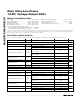
ELECTRICAL CHARACTERISTICS (continued)
(V
DD
= +1.8V to +5.5V, OUT_ unloaded, T
A
= T
MIN
to T
MAX
, unless otherwise noted. Typical values are at T
A
= +25°C.)
PARAMETER SYMBOL CONDITIONS MIN TYP MAX UNITS
DAC OUTPUTS (OUTA, OUTB)
Capacitive Driving Capability C
L
1000 pF
V
DD
= 5V, V
OUT
set to full scale, OUT
shorted to GND, source current
65
V
DD
= 5V V
OUT
set to 0V, OUT shorted to
V
DD
, sink current
65
V
DD
= 1.8V, V
OUT
set to full scale OUT
shorted to GND, source current
14
Short-Circuit Current (Note 6)
V
DD
= 1.8V, V
OUT
set to 0V, OUT shorted to
V
DD
, sink current
14
mA
V
DD
= 5V 3
Coming out of shutdown
(MAX5532/MAX5534)
V
DD
= 1.8V 3.8
DAC Power-Up Time
Coming out of standby
(MAX5533/MAX5535)
V
DD
= 1.8V
to 5.5V
0.4
µs
Output Power-Up Glitch C
L
= 100pF 10 mV
FB_ Input Current 10 pA
DIGITAL INPUTS (SCLK, DIN, CS)
4.5V ≤ V
DD
≤ 5.5V 2.4
2.7V < V
DD
≤ 3.6V 2.0Input High Voltage V
IH
1.8V ≤ V
DD
≤ 2.7V 0.7 x V
DD
V
4.5V ≤ V
DD
≤ 5.5V 0.8
2.7V < V
DD
≤ 3.6V 0.6
Input Low Voltage V
IL
1.8V ≤ V
DD
≤ 2.7V 0.3 x V
DD
V
Input Leakage Current I
IN
(Note 9) ±0.05 ±0.5 µA
Input Capacitance C
IN
10 pF
DYNAMIC PERFORMANCE
Voltage-Output Slew Rate SR Positive and negative (Note 10) 10 V/ms
Voltage-Output Settling Time
0.1 to 0.9 of full scale to within 0.5 LSB
(Note 10)
660 µs
V
DD
= 5V 80
0.1Hz to 10Hz
V
DD
= 1.8V 55
V
DD
= 5V 620
Output Noise Voltage
10Hz to 10kHz
V
DD
= 1.8V 476
µV
P-P