
Datasheet


V
DD
, V
LOGIC
, CS, SCLK, DIN to GND......................-0.3V to +6V
H_, L_, and W_ to GND ..............................-0.3V to (V
DD
+ 0.3V)
DOUT to GND.............................................-0.3V to (V
DD
+ 0.3V)
AGND to GND .......................................................-0.3V to +0.3V
Input and Output Latchup Immunity...............................±200mA
Maximum Continuous Current into H_, L_, and W_.........±500µA
Continuous Power Dissipation (T
A
= +70°C)
16-Pin QSOP (derate 8.3mW/°C above +70°C)........666.7mW
16-Pin QFN (derate 18.5mW/°C above +70°C) .........1481mW
Operating Temperature Range ...........................-40°C to +85°C
Storage Temperature Range .............................-60°C to +150°C
Maximum Junction Temperature .....................................+150°C
Lead Temperature (soldering, 10s) .................................+300°C
MAX5408–MAX5411
Dual, Audio, Log Taper Digital Potentiometers
2 _______________________________________________________________________________________
ABSOLUTE MAXIMUM RATINGS
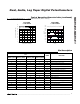
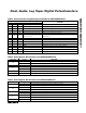
ELECTRICAL CHARACTERISTICS
(V
DD
= +2.7V to +3.6V (MAX5408/MAX5409), V
DD
= +4.5V to +5.5V (MAX5410/MAX5411), V
H_
= V
DD
, V
L_
= 0, T
A
= T
MIN
to T
MAX
.
Typical values are at T
A
= +25°C, unless otherwise specified.)
Stresses beyond those listed under “Absolute Maximum Ratings” may cause permanent damage to the device. These are stress ratings only, and functional
operation of the device at these or any other conditions beyond those indicated in the operational sections of the specifications is not implied. Exposure to
absolute maximum rating conditions for extended periods may affect device reliability.
PARAMETER SYMBOL CONDITIONS MIN TYP MAX UNITS
End-to-End Resistance 71013kΩ
Maximum Bandwidth (Note 1) C
W_
= 50pF 100 kHz
Absolute Tolerance ±0.25 dB
Tap-to-Tap Tolerance ±0.1 dB
Total Harmonic Distortion + Noise THD+N V
IN
= 1V
RMS
, f = 1kHz, tap = -6dB 0.002 %
Channel Isolation -100 dB
Interchannel Matching f = 20Hz to 20kHz, tap = -6dB ±0.5 dB
Mute Attenuation -90 dB
Power-Supply Rejection Ratio PSRR -80 dB
Wiper Resistance R
W
1000 1700 Ω
Wiper Capacitance C
W
10 pF
Digital Clock Feedthrough f
SCLK
= 20Hz to 20kHz, tap = -6dB -90 dB
End-to-End Resistance
Temperature Coefficient
35 ppm/°C
Ratiometric Resistance
Temperature Coefficient
5 ppm/°C
DIGITAL INPUTS (V
LOGIC
> 4.5V)
Input High Voltage V
IH
2.4 V
Input Low Voltage V
IL
0.8 V
Input Leakage Current ±1 µA
Input Capacitance 5pF
DIGITAL INPUTS (V
LOGIC
< 4.5V)
Input High Voltage V
IH
0.7 x
V
LOGIC
V
Input Low Voltage V
IL
0. 3 x
V
LOGIC
V
Input Leakage Current ±1 µA
Input Capacitance 5pF