
Datasheet


Dual, 256-Tap, Volatile, Low-Voltage,
Linear Taper Digital Potentiometer
MAX5392
10 _____________________________________________________________________________________
Detailed Description
The MAX5392 dual, 256-tap, volatile, low-voltage linear
taper digital potentiometer offers three end-to-end resis-
tance values of 10kI, 50kI, and 100kI. The potenti-
ometer consists of 255 fixed resistors in series between
terminals H_ and L_. The potentiometer wiper, W_, is
programmable to access any one of the 256 tap points
on the resistor string.
The potentiometers are programmable independently of
each other. The MAX5392 features an I
2
C interface.
Charge Pump
TThe MAX5392 contains an internal charge pump that
guarantees the maximum wiper resistance, R
WL
, to be
less than 200Ω for supply voltages down to 1.7V. Pins
H_, W_, and L_ are still required to be less than V
DD
+
0.3V. A bypass input, BYP, is provided to allow addi-
tional filtering of the charge-pump output, further reduc-
ing clock feedthrough that can occur on H_, W_, or L_.
The nominal clock rate of the charge pump is 600kHz.
BYP should remain resistively unloaded as any addi-
tional load would increase clock feedthrough. See the
Charge-Pump Feedthrough at W_ vs. C
BYP
graph in the
Typical Operating Characteristics for C
BYP
sizing guide-
lines with respect to clock feedthrough to the wiper. The
value of C
BYP
does affect the startup time of the charge
pump; however, C
BYP
does not impact the ability to
communicate with the device, nor is there a minimum
C
BYP
requirement. The maximum wiper impedance
specification is not guaranteed until the charge pump is
fully settled. See the BYP Ramp Time vs. C
BYP
graph in
the Typical Operating Characteristics for C
BYP
impact on
charge-pump settling time.
I
2
C Digital Interface
The I
2
C interface contains a shift register that decodes
the command and address bytes, routing the data to the
appropriate control registers. Data written to a control
register immediately updates the wiper position. The
wipers A and B power up in midposition, D[7:0] = 80h.
Serial Addressing
The MAX5392 operates as a slave device that receives
data through an I
2
C/SMBusK-compatible 2-wire serial
interface. The interface uses a serial-data access line
(SDA) and a serial-clock line (SCL) to achieve bidirec-
tional communication between master(s) and slave(s).
A master, typically a microcontroller, initiates all data
transfers to the port and generates the SCL clock that
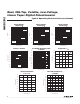
synchronizes the data transfer. See Figure 2. Connect a
pullup resistor, typically 4.7kI, between each of the SDA
and SCL lines to a voltage between V
DD
and 5.5V.
SMBus is a trademark of Intel Corp.
Figure 2. I
2
C Serial-Interface Timing Diagram
SDA
SCL
START
CONDITION
(S)
t
LOW
t
BUF
t
HIGH
t
HD:STA
t
HD:STA
t
SU:DAT
t
R
t
F
t
SU:STD
REPEATD
START CONDITION
(Sr)
ACKNOWLEDGE (A) STOP CONDITION
(P)
START CONDITION
(S)
t
HD:DAT
t
SU:DTA