
Datasheet


Dual, 256-Tap, Volatile, Low-Voltage,
Linear Taper Digital Potentiometer
MAX5392
_______________________________________________________________________________________ 9
Pin Description
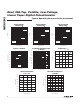
Pin Configuration
16
15
14
13
12
11
10
1
2
3
4
5
6
7
V
DD
N.C.
SCL
SDAHB
LA
WA
HA
TOP VIEW
MAX5392
A0
A1
A2BYP
LB
98 GNDI.C.
WB
+
TSSOP
PIN NAME FUNCTION
1 HA
Resistor A High Terminal. The voltage at HA can be higher or lower than the voltage at LA. Current
can flow into or out of HA.
2 WA Resistor A Wiper Terminal
3 LA
Resistor A Low Terminal. The voltage at LA can be higher or lower than the voltage at HA. Current
can flow into or out of LA.
4 HB
Resistor B High Terminal. The voltage at HB can be higher or lower than the voltage at LB. Current
can flow into or out of HB.
5 WB Resistor B Wiper Terminal
6 LB
Resistor B Low Terminal. The voltage at LB can be higher or lower than the voltage at HB. Current
can flow into or out of LB.
7 BYP
Internal Power-Supply Bypass. For additional charge-pump filtering, bypass to GND with a capaci-
tor close to the device.
8 I.C. Internally Connected. Connect to GND.
9 GND Ground
10 A2 Address Input 2. Connect to V
DD
or GND.
11 A1 Address Input 1. Connect to V
DD
or GND.
12 A0 Address Input 0. Connect to V
DD
or GND.
13 SDA I
2
C-Compatible Serial-Data Input/Output. A pullup resistor is required.
14 SCL I
2
C-Compatible Serial-Clock Input. A pullup resistor is required.
15 N.C. No Connection. Not internally connected.
16 V
DD
Power-Supply Input. Bypass V
DD
to GND with a 0.1FF capacitor close to the device.