
Datasheet


Dual, 256-Tap, Volatile, Low-Voltage,
Linear Taper Digital Potentiometer
MAX5392
4 ______________________________________________________________________________________
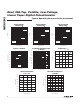
Figure 1. Voltage-Divider and Variable Resistor Configurations
ELECTRICAL CHARACTERISTICS (continued)
(V
DD
= +1.7V to +5.5V, V
H_
= V
DD
, V
L_
= 0, T
A
= T
MIN
to T
MAX
, unless otherwise noted. Typical values are at V
DD
= +1.8V,
T
A
= +25NC.) (Note 1)
Note 1: All devices are 100% production tested at T
A
= +25NC. Specifications over temperature limits are guaranteed by design
and characterization.
Note 2: DNL and INL are measured with the potentiometer configured as a voltage-divider (Figure 1) with H_ = V
DD
and L_ = GND.
The wiper terminal is unloaded and measured with a high-input-impedance voltmeter.
Note 3: R-DNL and R-INL are measured with the potentiometer configured as a variable resistor (Figure 1). DNL and INL are mea-
sured with the potentiometer configured as a variable resistor. H_ is unconnected and L_ = GND. For V
DD
= +5V, the wiper
terminal is driven with a source current of 400FA for the 10kI configuration, 80FA for the 50kI configuration, and 40FA for
the 100kI configuration. For V
DD
= +1.7V, the wiper terminal is driven with a source current of 150FA for the 10kI configu-
ration, 30FA for the 50kI configuration, and 15FA for the 100kI configuration.
Note 4: The wiper resistance is the worst value measured by injecting the currents given in Note 3 to W_ with L_ = GND.
R
W_
= (V
W_
- V
H_
)/I
W_
.
Note 5: Drive HA with a 1kHz GND to V
DD
amplitude tone. LA
= LB = GND. No load. WB is at midscale with a 10pF load. Measure
WB.
Note 6: The wiper-settling time is the worst-case 0 to 50% rise time, measured between tap 0 and tap 127. H_ = V
DD
, L_ = GND,
and the wiper terminal is loaded with 10pF capacitance to ground.
Note 7: Digital timing is guaranteed by design and characterization, not production tested.
Note 8: The SCL clock period includes rise and fall times (t
R
= t
F
). All digital input signals are specified with t
R
= t
F
= 2ns and timed
from a voltage level of (V
IL
+ V
IH
)/2.
Note 9: An appropriate bus pullup resistance must be selected depending on board capacitance. For I
2
C-bus specification infor-
mation from NXP Semiconductor (formerly Philips Semiconductor), refer to the UM10204: I
2
C-Bus Specification and User
Manual.
H
L
W W
N.C.
L
PARAMETER SYMBOL CONDITIONS MIN TYP MAX UNITS
Data Setup Time t
SU:DAT
100 ns
Data Hold Time t
HD:DAT
0
Fs
SDA, SCL Rise Time t
R
0.3
Fs
SDA, SCL Fall t
F
0.3
Fs
Setup Time for STOP Condition t
SU:STO
0.6
Fs
Bus Free Time Between STOP and
START Condition
t
BUF
Minimum power-up rate = 0.2V/Fs
1.3
Fs
Pulse Suppressed Spike Width t
SP
50 ns
Capacitive Load for Each Bus C
B
(Note 9) 400 pF