
Datasheet
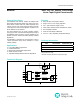

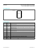

PIN NAME FUNCTION
1 HA
Resistor A High Terminal. The voltage at HA can be higher or lower than the voltage at LA. Current
can ow into or out of HA.
2 WA Resistor A Wiper Terminal
3 LA
Resistor A Low Terminal. The voltage at LA can be higher or lower than the voltage at HA. Current
can ow into or out of LA.
4 HB
Resistor B High Terminal. The voltage at HB can be higher or lower than the voltage at LB. Current
can ow into or out of HB.
5 WB Resistor B Wiper Terminal
6 LB
Resistor B Low Terminal. The voltage at LB can be higher or lower than the voltage at HB. Current
can ow into or out of LB.
7 I.C. Internally Connected. Connect to GND.
8 GND Ground
9 A2 Address Input 2. Connect to V
DD
or GND.
10 A1 Address Input 1. Connect to V
DD
or GND.
11 A0 Address Input 0. Connect to V
DD
or GND.
12 SDA I
2
C-Compatible Serial-Data Input/Output. A pullup resistor is required.
13 SCL I
2
C-Compatible Serial-Clock Input. A pullup resistor is required.
14 V
DD
Power-Supply Input. Bypass V
DD
to GND with a 0.1µF capacitor close to the device.
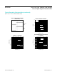
V
DD
SCL
SDA
HB
LA
WA
HA
+
A0
A1
A2
I.C.
LB
GND
WB
14
13
12
11
10
9
8
1
2
3
4
5
6
7
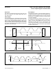
TOP VIEW
MAX5387
TSSOP
MAX5387 Dual, 256-Tap, Volatile, Low-Voltage
Linear Taper Digital Potentiometer
www.maximintegrated.com
Maxim Integrated
│
8
Pin Description
Pin Conguration