
Datasheet


(V
DD
= +2.6V to +5.5V, V
H_
= V
DD
, V
L_
= GND, T
A
= -40ºC to +125ºC, unless otherwise noted. Typical values are at V
DD
= +5V,
T
A
= +25ºC.) (Note 1)
Note 1: All devices are 100% production tested at T
A
= +25ºC. Specifications overtemperature limits are guaranteed by design and
characterization.
Note 2: DNL and INL are measured with the potentiometer configured as a voltage-divider (Figure 1) with H_ = V
DD
and L_ = 0V.
The wiper terminal is unloaded and measured with an ideal voltmeter.
Note 3: R-DNL and R-INL are measured with the potentiometer configured as a variable resistor (Figure 1). DNL and INL are mea-
sured with the potentiometer configured as a variable resistor. H_ is unconnected and L_ = GND. For V
DD
= +5V, the wiper
terminal is driven with a source current of 400µA for the 10kΩ configuration, 80µA for the 50kΩ configuration, and 40µA for
the 100kΩ configuration. For V
DD
= +2.6V, the wiper terminal is driven with a source current of 200µA for the 10kΩ configu-
ration, 40µA for the 50kΩ configuration, and 20µA for the 100kΩ configuration.
Note 4: The wiper resistance is the worst value measured by injecting the currents given in Note 3 into W_ with L_ = GND. R
W
=
(V
W
- V
H
)/I
W
.
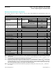
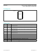
PARAMETER SYMBOL CONDITIONS MIN TYP MAX UNITS
AC PERFORMANCE
Crosstalk (Note 5) -90 dB
-3dB Bandwidth BW
Code = 80H,
10pF load,
V
DD
= +2.6V
MAX5387L 600
kHzMAX5387M 150
MAX5387N 75
Total Harmonic Distortion Plus
Noise
THD+N Measured at W; V
H_
= 1V
RMS
at 1kHz 0.015 %
Wiper Settling Time (Note 6) t
S
MAX5387L 300
nsMAX5387M 1000
MAX5387N 2000
POWER SUPPLIES
Supply-Voltage Range V
DD
2.6 5.5 V
Standby Current Digital inputs = V
DD
or GND 1 µA
DIGITAL INPUTS
Minimum Input High Voltage V
IH
70 % x V
DD
Maximum Input Low Voltage V
IL
30 % x V
DD
Input Leakage Current -1 +1 µA
Input Capacitance 5 pF
TIMING CHARACTERISTICS (Notes 7, 8)
Maximum SCL Frequency f
SCL
400 kHz
Setup Time for START Condition t
SU:STA
0.6 µs
Hold Time for START Condition t
HD:STA
0.6 µs
SCL High Time t
HIGH
0.6 µs
SCL Low Time t
LOW
1.3 µs
Data Setup Time t
SU:DAT
100 ns
Data Hold Time t
HD:DAT
0 µs
SDA, SCL Rise Time t
R
0.3 µs
SDA, SCL Fall t
F
0.3 µs
Setup Time for STOP Condition t
SU:STO
0.6 µs
Bus Free Time Between STOP and
START Conditions
t
BUF
Minimum power-up rate = 0.2V/µs 1.3 µs
Pulse-Suppressed Spike Width t
SP
50 ns
Capacitive Load for Each Bus C
B
400 pF
MAX5387 Dual, 256-Tap, Volatile, Low-Voltage
Linear Taper Digital Potentiometer
www.maximintegrated.com
Maxim Integrated
│
3
Electrical Characteristics (continued)