
Datasheet

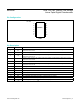

Bit Transfer
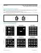
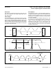
One data bit is transferred during each clock pulse. The
data on the SDA line must remain stable while SCL is
high. See Figure 4.
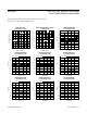
Acknowledge
The acknowledge bit is a clocked 9th bit that the recipi-
ent uses to handshake receipt of each byte of data. See
Figure 5. Each byte transferred requires a total of nine
bits. The master controller generates the 9th clock pulse,
and the recipient pulls down SDA during the acknowledge
clock pulse, so the SDA line remains stable low during the
high period of the clock pulse.
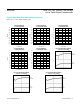
Slave Address
The MAX5387 includes a 7-bit slave address (Figure 6).
The 8th bit following the 7th bit of the slave address is the
NOP/W bit. Set the NOP/W bit low for a write command
and high for a no-operation command. The device does
not support readback.
The device provides three address inputs (A0, A1, and
A2), allowing up to eight devices to share a common bus
(Table 1). The first 4 bits (MSBs) of the factory-set slave
addresses are always 0101. A2, A1, and A0 set the next
3 bits of the slave address. Connect each address input
to V
DD
or GND. Each device must have a unique address
to share a common bus.
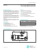
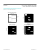
Figure 3. START and STOP Conditions
Figure 4. Bit Transfer
Figure 5. Acknowledge
P
STOP
CONDITION
S
START CONDITION
SDA
SCL
SDA
SCL
DATA STABLE,
DATA VALID
CHANGE OF
DATA ALLOWED
9821
START
CONDITION
SCL
SDA
CLOCK PULSE FOR
ACKNOWLEDGMENT
NOT ACKNOWLEDGE
ACKNOWLEDGE
MAX5387 Dual, 256-Tap, Volatile, Low-Voltage
Linear Taper Digital Potentiometer
www.maximintegrated.com
Maxim Integrated
│
10