
Datasheet


MAX536/MAX537
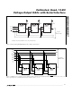
Using an AC Reference
In applications where the reference has AC signal compo-
nents, the MAX536/MAX537 have multiplying capability
within the reference input range specifications. Figure 12
shows a technique for applying a sine-wave signal to the
reference input where the AC signal is offset before being
applied to REFAB/REFCD. The reference voltage must
never be more negative than DGND.
The MAX536’s total harmonic distortion plus noise
(THD+N) is typically less than 0.012%, given a 5V
P-P
signal
swing and input frequencies up to 35kHz, or given a 2V
P-P
swing and input frequencies up to 50kHz. The typical -3dB
frequency is 700kHz as shown in the Typical Operating
Characteristics graphs.
For the MAX537, with an input signal amplitude of
0.85mV
P-P
, THD+N is typically less than 0.024% with a
5kΩ load in parallel with 100pF and input frequencies up
to 100kHz, or with a 2kΩ load in parallel with 100pF and
input frequencies up to 95kHz.
Offsetting AGND
AGND can be biased from DGND to the reference voltage
to provide an arbitrary nonzero output voltage for a zero
input code (Figure 13). The output voltage V
OUTA
is:
V
OUTA
= V
BIAS
+ N
B
(V
IN
)
where V
BIAS
is the positive offset voltage (with respect
to DGND) applied to AGND, and N
B
is the numeric
value of the DAC’s binary input code. Since AGND is
common to all four DACs, all outputs will be offset by
V
BIAS
in the same manner. As the voltage at AGND
increases, the DAC’s resolution decreases because its
full-scale voltage swing is effectively reduced. AGND
should not be biased more negative than DGND.
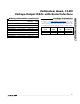
Power-Supply Considerations
On power-up, V
SS
should come up first, V
DD
next, then
REFAB or REFCD. If supply sequencing is not possible,
tie an external Schottky diode between V
SS
and AGND
as shown in Figure 14. On power-up, all input and DAC
registers are cleared (set to zero code) and SDO is in
Mode 0 (serial data is shifted out of SDO on the clock’s
rising edge).
For rated MAX536 performance, V
DD
should be 4V
higher than REFAB/REFCD and should be between
10.8V and 13.2V. When using the MAX537, V
DD
should
be at least 2.2V higher than REFAB/REFCD and should
be between 4.75V and 5.5V. Bypass both V
DD
and V
SS
with a 4.7µF capacitor in parallel with a 0.1µF capacitor
to AGND. Use short lead lengths and place the bypass
capacitors as close to the supply pins as possible.
Grounding and Layout Considerations
Digital or AC transient signals between AGND and
DGND can create noise at the analog outputs. Tie
AGND and DGND together at the DAC, then tie this
point to the highest quality ground available.
Good PCB ground layout minimizes crosstalk between
DAC outputs, reference inputs, and digital inputs.
Reduce crosstalk by keeping analog lines away from
digital lines. Wire-wrapped boards are not recommend-
ed.
Calibrated, Quad, 12-Bit
Voltage-Output DACs with Serial Interface
22 ______________________________________________________________________________________
MAX536
MAX537
1N5817
3
4
V
SS
AGND
Figure 14. When V
SS
and V
DD
cannot be sequenced, tie a
Schottky diode between V
SS
and AGND.