
Datasheet


MAX536/MAX537
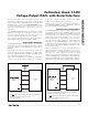
When daisy-chaining MAX536s, the delay from
CS
low to SCK high (t
CSS
) must be the greater of:
t
DV
+ t
DS
or
t
TR
+ t
RC
+ t
DS
- t
CSW
where t
RC
is the time constant of the external pullup resistor
(R
p
) and the load capacitance (C) at SDO. For t
RC
< 20ns,
t
CSS
is simply t
DV
+ t
DS
. Calculate t
RC
from the following
equation:
t
RC
= R
p
(C) ln
where V
PULLUP
is the voltage to which the pullup resistor is
connected.
Additionally, when daisy-chaining devices, the maximum
clock frequency is limited to:
1
f
SCK
(max) = ——————————————
2 (t
DO
+ t
RC
- 38ns + t
DS
)
For example, with t
RC
= 23ns (5V ±10% supply with
R
p
= 1kΩ and C = 30pF), the maximum clock frequency is
8.7MHz.
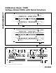
Figure 9 shows an alternate method of connecting sev
eral
MAX536/MAX537s. In this configuration, the data bus is
common to all devices; data is not shifted through a
daisy-chain. More I/O lines are required in this configu-
ration because a dedicated chip-select input (CS) is
required for each IC.
Calibrated, Quad, 12-Bit
Voltage-Output DACs with Serial Interface
16 ______________________________________________________________________________________
V
PULLUP
V
PULLUP
- 2.4V
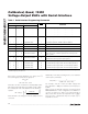
Table 1. Serial-Interface Programming Commands
“X” = Don’t Care. LDAC provides true latch control: when LDAC is low, the DAC registers are transparent; when LDAC is high,
the DAC registers are latched.
Mode 0, DOUT clocked out on SCK’s falling edge. All DACs
updated from their respective input registers.
Mode 1 (default condition at power-up), DOUT clocked out on
SCK’s rising edge. All DACs updated from their respective
input registers.
Load DAC D input register; DAC D is immediately updated.012-bit DAC data1X11
Load DAC C input register; DAC C is immediately updated.012-bit DAC data1X01
Load DAC B input register; DAC B is immediately updated.012-bit DAC data1X10
Load DAC A input register; DAC A is immediately updated.012-bit DAC data10 X0
XXXXXXXXXXXXX0101
XXXXXXXXXXXXX0111
Update all DACs from their respective input registers.1XXXXXXXXXXXX01X0
No operation (NOP)XXXXXXXXXXXXX001X
Load all DACs from shift register.X12-bit DAC data000X
Load input register D; all DAC registers updated.112-bit DAC data1111
Load input register C; all DAC registers updated.112-bit DAC data1101
Load input register B; all DAC registers updated.112-bit DAC data1110
Load input register A; all DAC registers updated.112-bit DAC data1100
Load DAC D input register; DAC output unchanged.112-bit DAC data1011
Load DAC C input register; DAC output unchanged.112-bit DAC data1001
Load DAC B input register; DAC output unchanged.112-bit DAC data1010
Load DAC A input register; DAC output unchanged.112-bit DAC data1000
D11…D0C0C1A0A1
FUNCTIONLDAC
16-BIT SERIAL WORD
()
[
]