
Datasheet


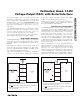


MAX536/MAX537
_______________Detailed Description
The MAX536/MAX537 contain four 12-bit voltage-output
DACs that are easily addressed using a simple 3-wire
serial interface. They include a 16-bit data-in/data-out
shift register, and each DAC has a double-buffered
input composed of an input register and a DAC register
(see the Functional Diagram on the front page).
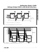
The DACs are “inverted” R-2R ladder networks that
convert 12-bit digital inputs into equivalent analog out-
put voltages in proportion to the applied reference-volt-
age inputs. DAC A and DAC B share the REFAB refer-
ence input, while DAC C and DAC D share the REFCD
reference input. The two reference inputs allow different
full-scale output voltage ranges for each pair of DACs.
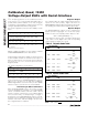
Figure 1 shows a simplified circuit diagram of one of
the four DACs.
Reference Inputs
The two reference inputs accept positive DC and AC
signals. The voltage at each reference input sets
the full-scale output voltage for its two correspond-
ing DACs. The REFAB/REFCD voltage range is 0V to
(V
DD
- 4V) for the MAX536 and 0V to (V
DD
- 2.2V) for the
MAX537. The output voltages V
OUT
_ are represented by
a digitally programmable voltage source as:
V
OUT_
= N
B
(V
REF)
/4096
where N
B
is the numeric value of the DAC’s binary input
code (0 to 4095) and V
REF
is the reference voltage.
Calibrated, Quad, 12-Bit
Voltage-Output DACs with Serial Interface
12 ______________________________________________________________________________________
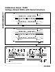
______________________________________________________________Pin Description
PIN NAME FUNCTION
OUTB DAC B Output Voltage
2 OUTA DAC A Output Voltage
3 V
SS
Negative Power Supply
AGND Analog Ground
5 REFAB Reference Voltage Input for DAC A and DAC B
6 DGND Digital Ground
7
LDAC
8 SDI Serial Data Input. Data is shifted into an internal 16-bit shift register on SCK's rising edge.
9
CS
10 SCK
11 SDO
12 REFCD Reference Voltage Input for DAC C and DAC D
13 TP Test Pin. Connect to V
DD
for proper operation.
14 V
DD
Positive Power Supply
15 OUTD DAC D Output Voltage
1
4
16 DAC C Output Voltage
Load DAC Input (active low). Driving this asynchronous input low transfers the contents of all input
registers to their respective DAC registers.
Chip-Select Input (active low). A low level on CS enables the input shift register and SDO.
On CS’s rising edge, data is latched into the appropriate register(s).
Shift Register Clock Input
Serial Data Output. SDO is the output of the internal shift register. SDO is enabled when CS is low.
For the MAX536, SDO is an open-drain output. For the MAX537, SDO has an active pullup to V
DD
.
OUTC
V
OUT
SHOWN FOR ALL 1s ON DAC
D0 D9 D10
D11
2R 2R 2R 2R
2R
RRR
REF
AGND
Figure 1. Simplified DAC Circuit Diagram