
Datasheet


MAX5352/MAX5353
Low-Power, 12-Bit Voltage-Output DACs
with Serial Interface
______________________________________________________________________________________ 13
The MAX5352’s total harmonic distortion plus noise
(THD+N) is typically less than -77dB (full-scale code),
and the MAX5353’s THD+N is typically less than
-72dB (full-scale code), given a 1Vp-p signal swing and
input frequencies up to 25kHz. The typical -3dB fre-
quency is 650kHz for both devices, as shown in the
Typical Operating Characteristics
graphs.
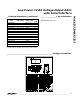
Digitally Programmable Current Source
The circuit of Figure 12 places an NPN transistor
(2N3904 or similar) within the op-amp feedback loop to
implement a digitally programmable, unidirectional cur-
rent source. The output current is calculated with the
following equation:
I
OUT
= (V
REF
/R) x (NB/4096)
where NB is the numeric value of the DAC’s binary
input code and R is the sense resistor shown in
Figure 12.
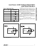
MAX5352
MAX5353
DAC
REF
OUT
FB
GND
+5V/+3.3V
V
DD
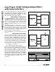
Figure 8. Unipolar Output Circuit
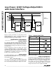
Table 3. Bipolar Code Table
MAX5352
MAX5353
DAC
REF
OUT
10k
10k
GND
+5V/+3.3V
V
DD
FB
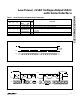
Figure 9. Unipolar Rail-to-Rail Output Circuit
ANALOG OUTPUT
1111 1111 1111 (0)
1000 0000 0001 (0)
DAC CONTENTS
MSB LSB
1000 0000 0000 (0) 0V
0111 1111 1111 (0)
0000 0000 0000 (0)
0000 0000 0001 (0)
+V
2047
2048
REF
+V
1
2048
REF
-V
1
2048
REF
-V
2047
2048
REF
-V
2048
2048
-V
REF REF
=
NOTE: ( ) are for sub-bit.