
Datasheet


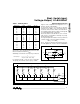


With the values of t
RC
given in Table 1, t
CSS0
is always
given by t
DV
+ t
DS
. For different values of R or C, t
RC
must be calculated to determine t
CSS0
.
Additionally, the maximum clock frequency is limited to
1
f
CLK
(max) = ————————————— .
2 x (t
DO
+ t
RC
-15ns + t
DS
)
For example, with t
RC
= 15ns (5V ±10% supply with
1kΩ pull-up), the maximum clock frequency is 2MHz.
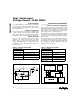
Digital-to-Analog Section
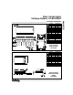
Figure 8 shows a simplified circuit diagram for one of
the DACs and the output amplifier.
A segmented scheme is used to improve linearity,
whereby the two MSBs of the 12-bit data word are
decoded to drive the three switches, SA, SB, and SC.
The remaining ten bits drive the switches S0 through S9
in a standard R-2R ladder configuration.
Each of the switches, SA, SB, and SC, steers 1/4 of the
total reference current with the remaining 1/4 passing
through the R-2R section.
The output amplifier and feedback resistor perform the
current-to-voltage conversion, giving the following:
VOUT_ = -D x VREF_,
where _ denotes A or B, and D is the fractional representa-
tion of the digital word. (D can be set from 0 to 4095/4096.)
MAX532
Dual, Serial-Input,
Voltage-Output, 12-Bit MDAC
______________________________________________________________________________________ 11
V
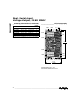
PULL-UP
(V) C (pF) R
P
(kΩ)t
RC
(ns)
4.5 20 1 15
4.5 35 1 27
4.5 50 1 38
4.5 100 1 76
4.5 150 1 114
11.4 20 3 14
11.4 35 3 25
11.4 50 3 35
11.4 100 3 71
11.4 150 3 106
13.5 20 3 12
13.5 35 3 21
13.5 50 3 29
13.5 100 3 59
13.5 150 3 88
Table 1. t
RC
Delay Times
RR R
2R 2R 2R 2R 2R 2R 2R
SC SB SA S9 S8 S0
R/2
RFB_
VOUT_
AGND_
SHOWN FOR ALL 1s ON DAC
VREF_
Figure 8. Simplified D/A Circuit Diagram
DACA
AGNDAV
SS
DGND
RFBA
VOUTA
V
OUT
V
IN
-12V to -15V
V
DD
VREFA
+12V to +15V
MAX532
Figure 9. Unipolar Binary Operation