
Datasheet
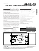


MAX5322
±10V, Dual, 12-Bit, Serial, Voltage-Output DAC
2 _______________________________________________________________________________________
ABSOLUTE MAXIMUM RATINGS
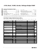
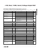
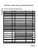
ELECTRICAL CHARACTERISTICS (DUAL SUPPLY)
(V
DD
= +15V ±5%, V
SS
= -15V ±5%, V
CC
= +5V ±10%, AGND = DGND = SGND_ = 0V, V
REF_
= 5V, R
LOAD
= 2kΩ, C
LOAD
= 250pF,
T
A
= T
MIN
to T
MAX
, unless otherwise noted. Typical values are at T
A
= +25°C.)
Stresses beyond those listed under “Absolute Maximum Ratings” may cause permanent damage to the device. These are stress ratings only, and functional
operation of the device at these or any other conditions beyond those indicated in the operational sections of the specifications is not implied. Exposure to
absolute maximum rating conditions for extended periods may affect device reliability.
V
DD
to AGND..........................................................-0.3V to +17V
V
SS
to AGND ..........................................................-17V to +0.3V
V
DD
to V
SS
..........................................................................+34V
V
CC
to DGND ...........................................................-0.3V to +6V
AGND to DGND.....................................................-0.3V to +0.3V
SGND_ to AGND ...................................................-0.3V to +0.3V
SCLK, DIN, CS, SHDN, UNI/BIP_, CLR,
LDAC, DOUT to DGND ..........................-0.3V to (V
CC
+ 0.3V)
OUT_ to AGND.................................(V
SS
- 0.3V) to (V
DD
+ 0.3V)
REF_ to AGND..........................................................-0.3V to +6V
Maximum Current into REF_ .............................................±10mA
Maximum Current into Any Pin Excluding REF_...............±50mA
Continuous Power Dissipation (T
A
= +70°C)
28-Pin SSOP (derate 9.5mW/°C above +70°C) ........761.9mW
Operating Temperature Range ...........................-40°C to +85°C
Junction Temperature......................................................+150°C
Storage Temperature Range .............................-65°C to +150°C
Lead Temperature (soldering, 10s) .................................+300°C
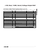
PARAMETER SYMBOL CONDITIONS MIN TYP MAX UNITS
STATIC ACCURACY
Resolution N 12 Bits
Integral Nonlinearity INL ±1 LSB
Differential Nonlinearity DNL Guaranteed monotonic ±1 LSB
Bipolar, code = 800hex ±2
Zero-Scale Error
Unipolar, code = 000hex ±2
LSB
Bipolar 0.9
Zero-Scale Temperature
Coefficient
Unipolar 0.09
ppm
FSR/°C
Bipolar (output unloaded) ±2
Gain Error
Unipolar (output unloaded) ±2
LSB
Bipolar (output unloaded) 2
Gain-Error Temperature
Coefficient
Unipolar (output unloaded) 2
ppm
FSR/°C
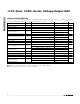
ANALOG OUTPUTS (OUTA, OUTB)
Output Voltage Range (V
SS
+ 1.5V) < V
OUT
< (V
DD
- 1.5V)
-2 x
V
REF
+2 x
V
REF
V
Resistive Load to GND R
LOAD
2kΩ
Capacitive Load to GND C
LOAD
250 pF
DC Output Resistance 0.5 Ω
SGND INPUTS (SGNDA, SGNDB)
Input Impedance 92 kΩ
REFERENCE INPUTS (REFA, REFB)
Reference Voltage Input Range 2.00 5.25 V
Input Resistance R
REF
Code = 555hex, worst-case code 15 22 kΩ
Reference Bandwidth V
REF
= 200mV
P-P
+ 5V
DC
200 kHz